Transistor that employs collective magnetic effects thereby providing improved energy efficiency

a technology of collective magnetic effects and transistors, applied in the field of transistors, can solve the problems of large power consumption and loss of logic state, and achieve the effects of increasing increasing the critical current, and decreasing the strength of the magnetic orientation

Active Publication Date: 2017-04-13
BOARD OF REGENTS
View PDF2 Cites 16 Cited by
  • Summary
  • Abstract
  • Description
  • Claims
  • Application Information

AI Technical Summary

Benefits of technology

[0009]In another embodiment of the present invention, a transistor comprises an easy-plane ferromagnetic film with an orientation along an easy axis within a plane of a ferromagnetic driven by vertical charge transport through a first and a second magnetic stack, where the easy-plane ferromagnetic film comprises two or more regions each of which individually approximates a macrospin. The transistor further comprises the first magnetic stack comprising a first and a second non-magnetic layer surrounding the easy-plane ferromagnetic film, where the first magnetic stack further comprises a first and a second easy-plane ferromagnetic layer on an outside of the first and second non-magnetic layers. The transistor additionally comprises the second magnetic stack comprising a third and a fourth non-magnetic layer surrounding the easy-plane ferromagnetic film, where the second magnetic stack further comprises a third and a fourth ferromagnetic layer with perpendicular anisotropy on an outside of the third and fourth non-magnetic layers. Furthermore, the transistor comprises input terminals connected to the first and second ferromagnetic layers of the first magnetic stack. Additionally, the transistor comprises output terminals connected to the third and fourth ferromagnetic layers of the second magnetic stack. An output current of the transistor is controlled via an input

Problems solved by technology

Only momentarily during switching between on and off states is power consumption large.
Another characteristic of CMOS is that it is v

Method used


Image

  • Transistor that employs collective magnetic effects thereby providing improved energy efficiency
  • Transistor that employs collective magnetic effects thereby providing improved energy efficiency
  • Transistor that employs collective magnetic effects thereby providing improved energy efficiency

Examples


Embodiment Construction

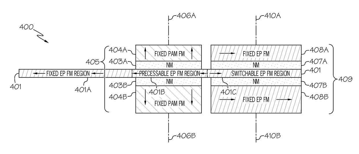
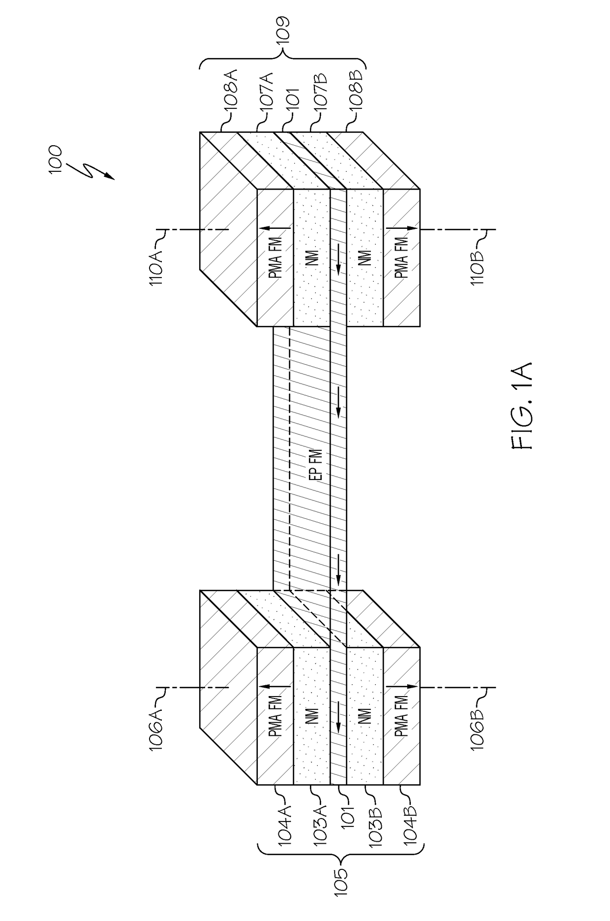
[0022]The principles of the present invention include two embodiments of a common transistor theme, referred to herein as the “Bi-Stack Magnetic Transistor” (BiSMaT). Both embodiments of the BiSMaT are intended to allow lower voltage, lower power memory and logic operation than possible with currently used complementary metal oxide semiconductor (CMOS) field-effect transistor (FET) based logic. Increased energy efficiency is not only important for its own sake, but also is necessary in logic circuits to enable increased device packing density and the resulting increase in computational power. Recent progress in the growth of magnetic thin films has made it possible to construct circuits in which materials with perpendicular and in-plane magnetic anisotropy are flexibly combined. This progress has improved prospects for the experimental realization of a new class of effects in spintronics in which collective magnetic degrees of freedom play a more active role than they do in memory d...


PUM


Abstract

A device or class of devices that provides a mechanism for controlling charge current flow in transistors that employs collective magnetic effects to overcome voltage limitations associated with single-particle thermionic emission as in conventional MOSFETs. Such a device may include two or more magnetic stacks with an easy-in-plane ferromagnetic film sandwiched between oppositely magnetically oriented perpendicular magnetization anisotropy (PMA) ferromagnets. Each stack includes two non-magnetic layers separating the easy-plane ferromagnetic film from the PMA layers. Charge current flow through one of these stacks controls the current-voltage negative differential resistance characteristics of the second stack through collective magnetic interactions. This can be exploited in a variety of digital logic gates consuming less energy than conventional CMOS integrated circuits. Furthermore, the easy-in-plane magnetic films may be subdivided into regions coupled through exchange interactions and the in-plane fixed magnetic layers in the input magnetic stacks can be used in non-volatile logic and memory.

Description

TECHNICAL FIELD[0001]The present invention relates generally to transistors, and more particularly to a transistor that employs collective magnetic effects to overcome voltage limitations associated with single-particle thermionic emission as in complementary metal oxide semiconductor (CMOS) field-effect transistor (FET) based logic thereby providing improved energy efficiency as well as to a transistor with a non-volatile memory capability for memory or non-volatile logic applications.BACKGROUND[0002]Complementary metal oxide semiconductor (CMOS) technology, employing complementary n-channel and p-channel metal-oxide-semiconductor field-effect transistors (MOSFETs), is a technology for constructing integrated circuits. CMOS technology is used in microprocessors, microcontrollers, static RAM, and other digital logic circuits. CMOS technology is also used for analog circuits, such as image sensors (e.g., CMOS sensor), data converters, and highly integrated transceivers for many types...

Claims


Application Information

Patent Timeline
IPC IPC(8): H01L43/06H01L43/10H01L43/04
CPCH01L43/065H01L43/10H01L43/04G11C11/161H03K19/18H10N50/10H10N52/101H10N50/85H10N52/80
Inventor BANERJEE, SANJAY K.MACDONALD, ALLANREGISTER, II, LEONARD FRANKLINTUTUC, EMANUELSODEMANN, INTICHEN, HUAMOU, XUEHAO
Owner BOARD OF REGENTS
Why Eureka
Try Eureka