

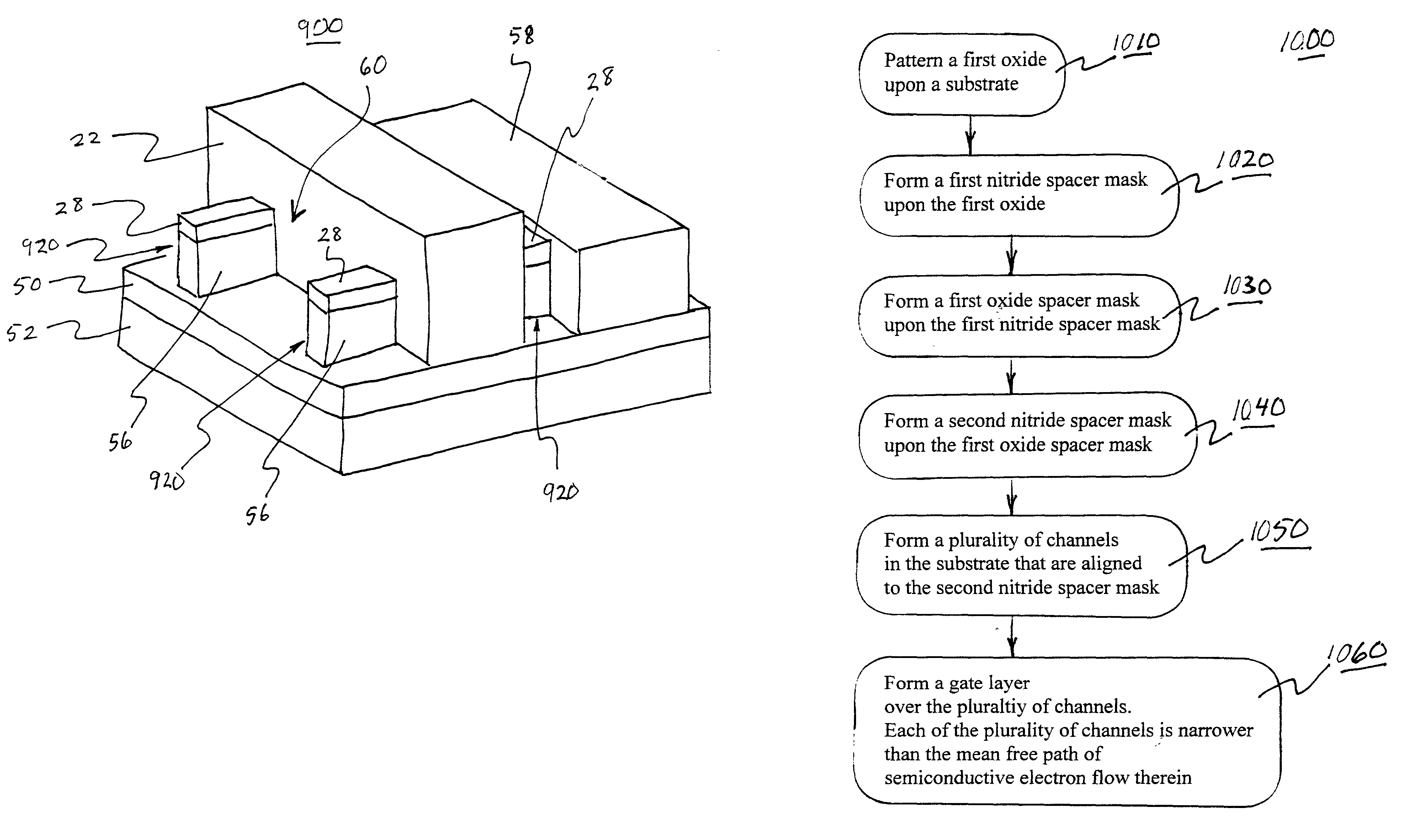
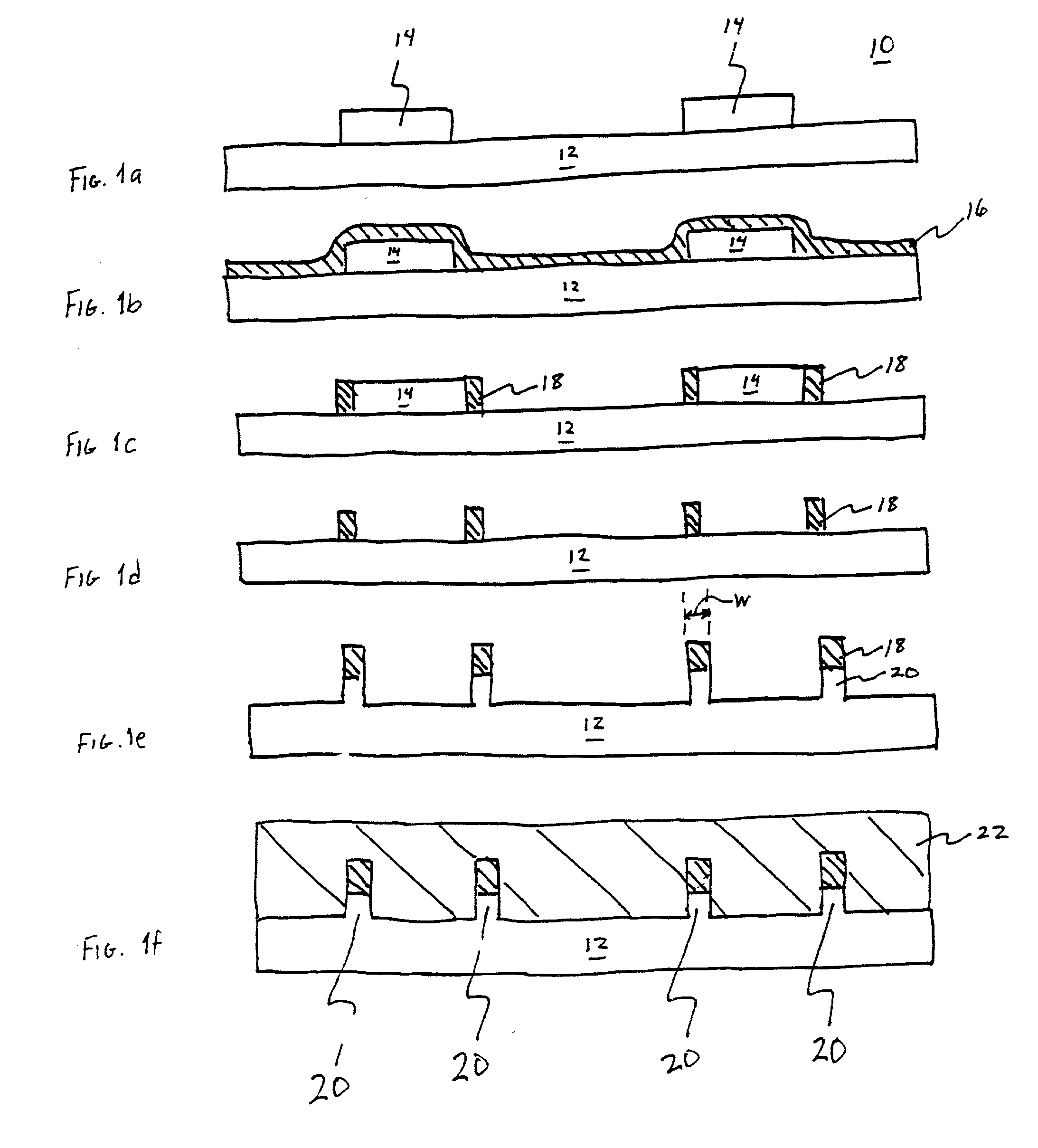
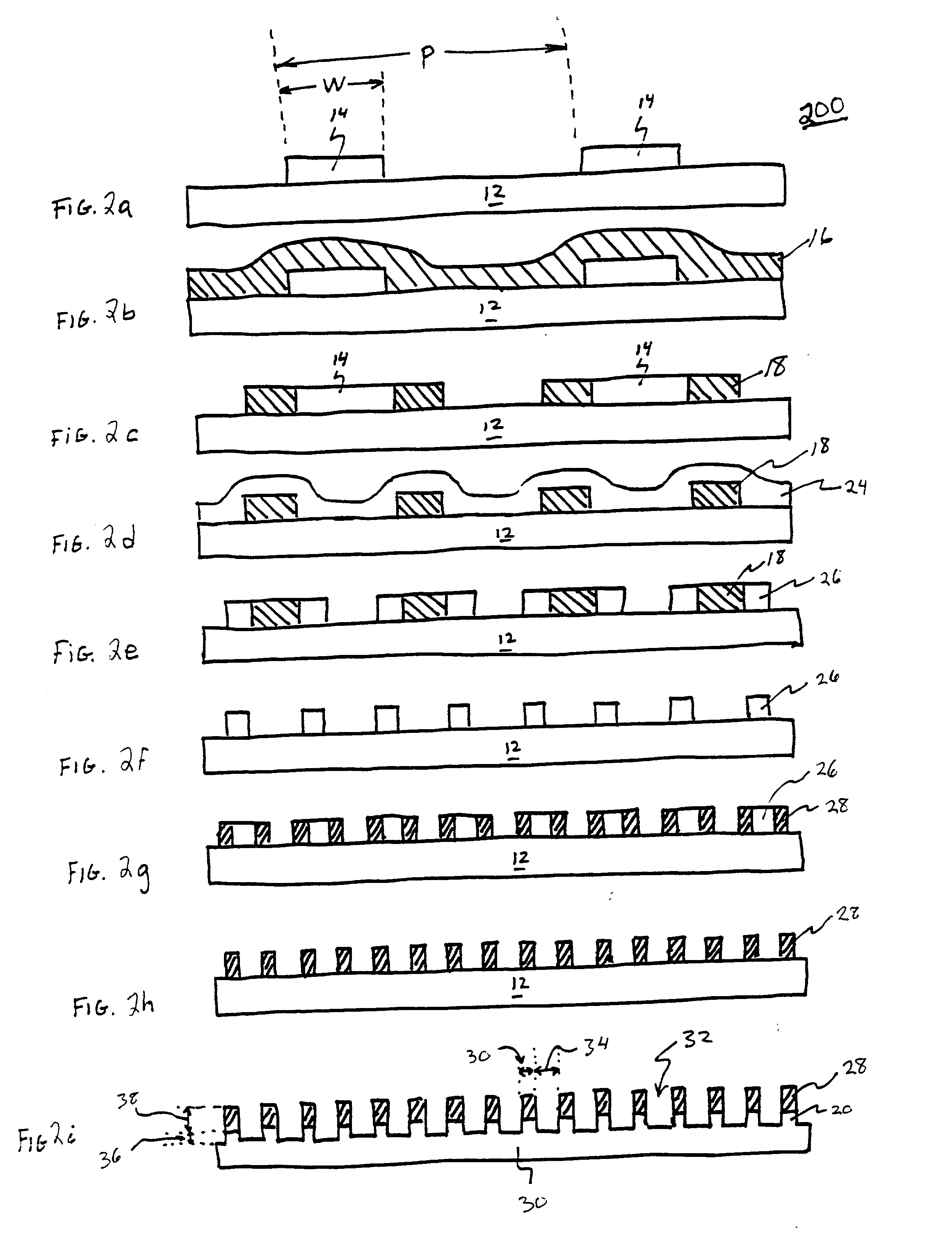
Quantum wire gate device and method of making same
a quantum wire gate and gate technology, applied in the field of integrated circuit fabrication, can solve the problems of increasing the length of the electron path, affecting the effective transition time, and unable to achieve the acceptable performance of 0.7x scaling,
- Summary
- Abstract
- Description
- Claims
- Application Information
AI Technical Summary
Problems solved by technology
Method used
Image

Examples
Embodiment Construction
[0064] William E. Alford, Reg. No. 37,764; Farzad E. Amini, Reg. No. P42,261; Aloysius T. C. AuYeung, Reg. No. 35,432; William Thomas Babbitt, Reg. No. 39,591; Carol F. Barry, Reg. No. 41,600; Jordan Michael Becker, Reg. No. 39,602; Bradley J. Bereznak, Reg. No. 33,474; Michael A. Bernadicou, Reg. No. 35,934; Roger W. Blakely, Jr., Reg. No. 25,831; Gregory D. Caldwell, Reg. No. 39,926; Ronald C. Card, Reg. No. 44,587; Andrew C. Chen, Reg. No. 43,544; Thomas M. Coester, Reg. No. 39,637; Alin Corie, Reg. No. P46,244; Dennis M. deGuzman, Reg. No. 41,702; Stephen M. De Klerk, under 37 C.F.R. .sctn.10.9(b); Michael Anthony DeSanctis, Reg. No. 39,957; Daniel M. De Vos, Reg. No. 37,813; Robert Andrew Diehl, Reg. No. 40,992; Sanjeet Dutta, Reg. No. P46,145; Matthew C. Fagan, Reg. No. 37,542; Tarek N. Fahmi, Reg. No. 41,402; Paramita Ghosh, Reg. No. 42,806; James Y. Go, Reg. No. 40,621; James A. Henry, Reg. No. 41,064; Willmore F. Holbrow III, Reg. No. P41,845; Sheryl Sue Holloway, Reg. No. ...
PUM
| Property | Measurement | Unit |
|---|---|---|
| width | aaaaa | aaaaa |
| width | aaaaa | aaaaa |
| width | aaaaa | aaaaa |
Abstract
Description
Claims
Application Information