Semiconductor laser device
a laser device and semiconductor technology, applied in semiconductor lasers, laser details, electrical equipment, etc., can solve the problems of high device differential resistance at working current, semiconductor laser device cannot work at a high temperature of 70.degree. c. or higher, and achieve the effect of reducing the loss of waveguides
- Summary
- Abstract
- Description
- Claims
- Application Information
AI Technical Summary
Benefits of technology
Problems solved by technology
Method used
Image
Examples
example 1
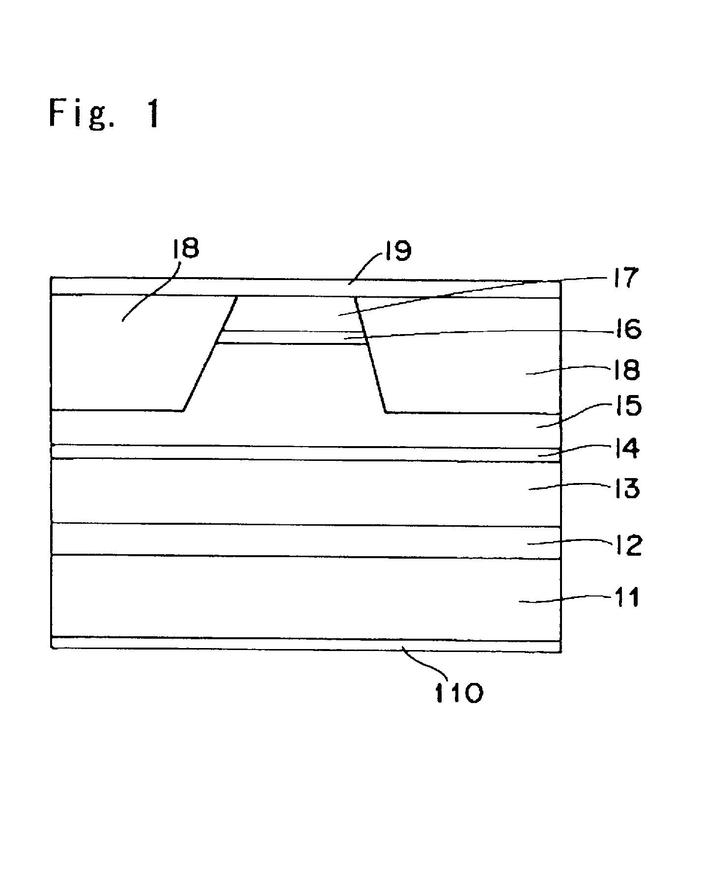
[0032] First, an Example of a self-excited oscillation type red semiconductor laser device to which the present invention is applied is illustrated with referring to FIG. 1. The semiconductor laser device of FIG. 1 has an n-type GaAs substrate 11, and a semiconductor laminate structure including a plurality of semiconductor layers which is epitaxially grown thereon.
[0033] The semiconductor laminate structure includes, in an order from a substrate 11, an n-type GaAs buffer layer (n-type impurity: Si, impurity concentration: 1.times.10.sup.18 cm.sup.-3, thickness: 200 nm) 12, an n-type (Al.sub.0.7Ga.sub.0.3).sub.0.5In.sub.0.5P first cladding layer (n-type impurity: Si, impurity concentration: 1.3.times.10.sup.18 cm.sup.-3, thickness: 1200 nm) 13, a GaInP active layer 14, and a p-type (Al.sub.0.7Ga.sub.0 3).sub.0.5In.sub.0.5P second cladding layer (p-type impurity: Be, impurity concentration: 1.3.times.10.sup.18 cm.sup.-3, thickness: 1200 nm) 15.
[0034] In this Example, the second cladd...
example 2
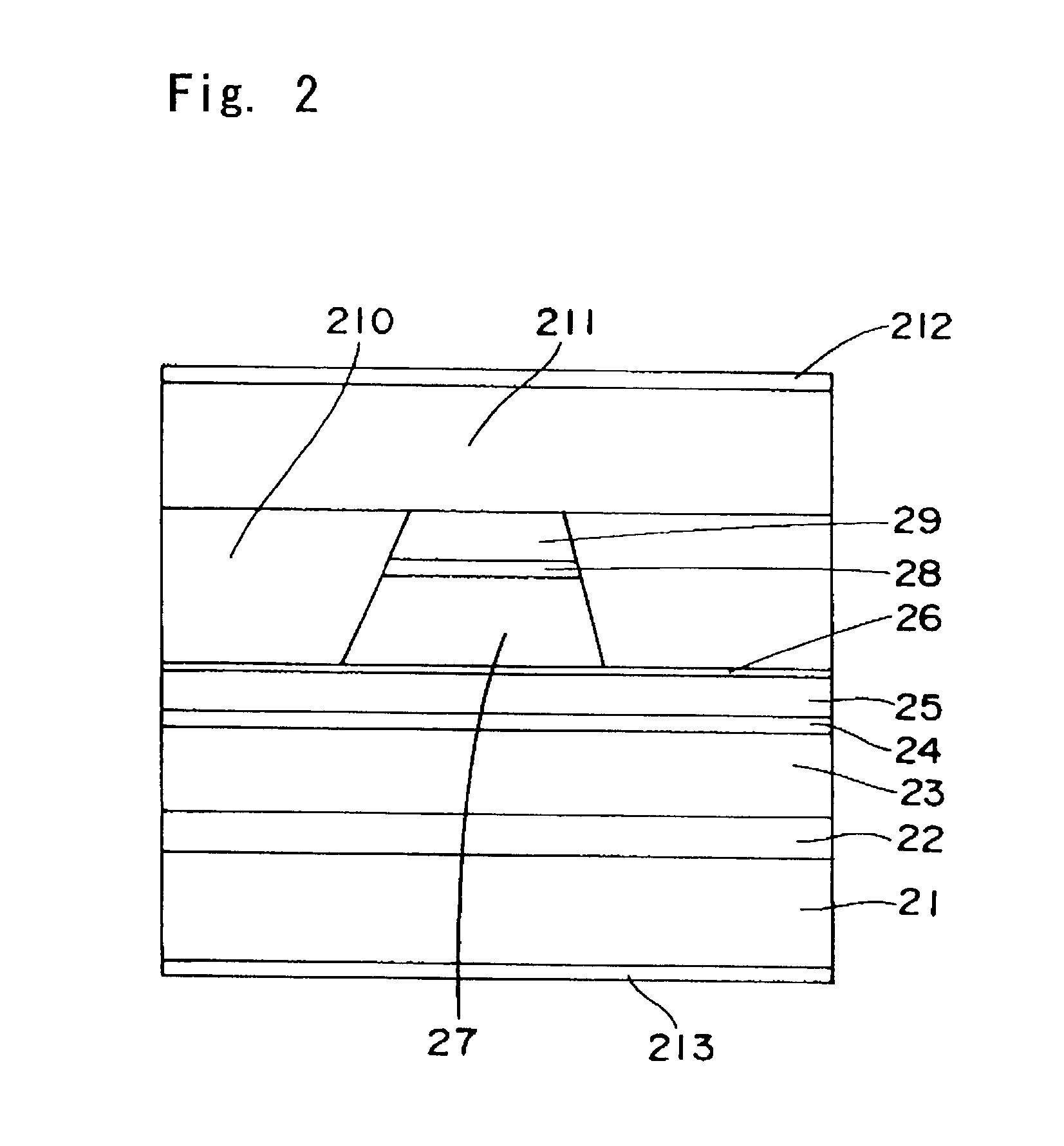
[0041] The second Example of an AlGaInP-series self-excited oscillation type red semiconductor laser device to which the present invention is applied is illustrated with referring to FIG. 2.
[0042] The semiconductor laser device of FIG. 2 has an n-type GaAs substrate 21, and a semiconductor laminate structure including a plurality of semiconductor layers which is epitaxially grown thereon.
[0043] The semiconductor laminate structure includes, in an order from a substrate 21, an n-type GaAs buffer layer (n-type impurity: Si, impurity concentration: 1.times.10.sup.18 cm.sup.-3, thickness: 200 nm) 22, an n-type (Al.sub.0.7Ga.sub.0.3).sub.0.5In.sub.0.5P first cladding layer (n-type impurity: Si, impurity concentration: 1.times.10.sup.18 cm.sup.-3, thickness: 1200 nm) 23, an MQW active layer 24, a p-type (Al.sub.0.7Ga.sub.0.3).sub.0.5In.sub.0.5P second cladding layer (p-type impurity: Be, impurity concentration: 1.0.times.10.sup.18 cm.sup.-3, thickness: 2500 nm) 25, a GaInP etch stop layer...
example 3
[0050] The third Example of an AlGaInP-series self-excited oscillation red semiconductor laser device to which the present invention is applied is illustrated with referring to FIG. 3.
[0051] Differences from the second Example (FIG. 2) are that the impurity concentration in a third cladding layer 37 was made to be 1.3.times.10.sup.18 cm.sup.-3 only in the region of 30 nm thickness from the interface with a p-type GaInP intermediate layer 38 and that it was lowered to 1.0.times.10.sup.18 cm.sup.-3 in other regions. When the impurity concentration of the p-type cladding layer is made to be high, the impurity Be becomes easy to diffuse and, when the impurity diffuses to the active layer, the device property is deteriorated, such as an increase in a threshold and a decrease in the efficacy. Therefore, it is desirable that the region having a high Be concentration in the cladding layer is separated from the active layer to the atmost.
[0052] Also, in this Example, in devices in which the ...
PUM
 Abstract
Description
Claims
Application Information


