Plasmonic nanophotonics methods, materials, and apparatuses

a technology of plasmonic nanophotonics and materials, applied in the direction of logic circuits, pulse techniques, instruments using specific components, etc., can solve the problems of device not being able to perform optical circuiting, optical switching, selective optical transmission,

Inactive Publication Date: 2003-03-06
NEW MEXICO STATE UNIV TECH TRANSFER
View PDF22 Cites 85 Cited by
  • Summary
  • Abstract
  • Description
  • Claims
  • Application Information

AI Technical Summary

Problems solved by technology

However, all the devices described require holes (or modulation in the metal film) to be periodic.
The device is not capable of optical circuiting, optical switching, or selective optical transmission.

Method used


Image

  • Plasmonic nanophotonics methods, materials, and apparatuses
  • Plasmonic nanophotonics methods, materials, and apparatuses
  • Plasmonic nanophotonics methods, materials, and apparatuses

Examples


Embodiment Construction

)

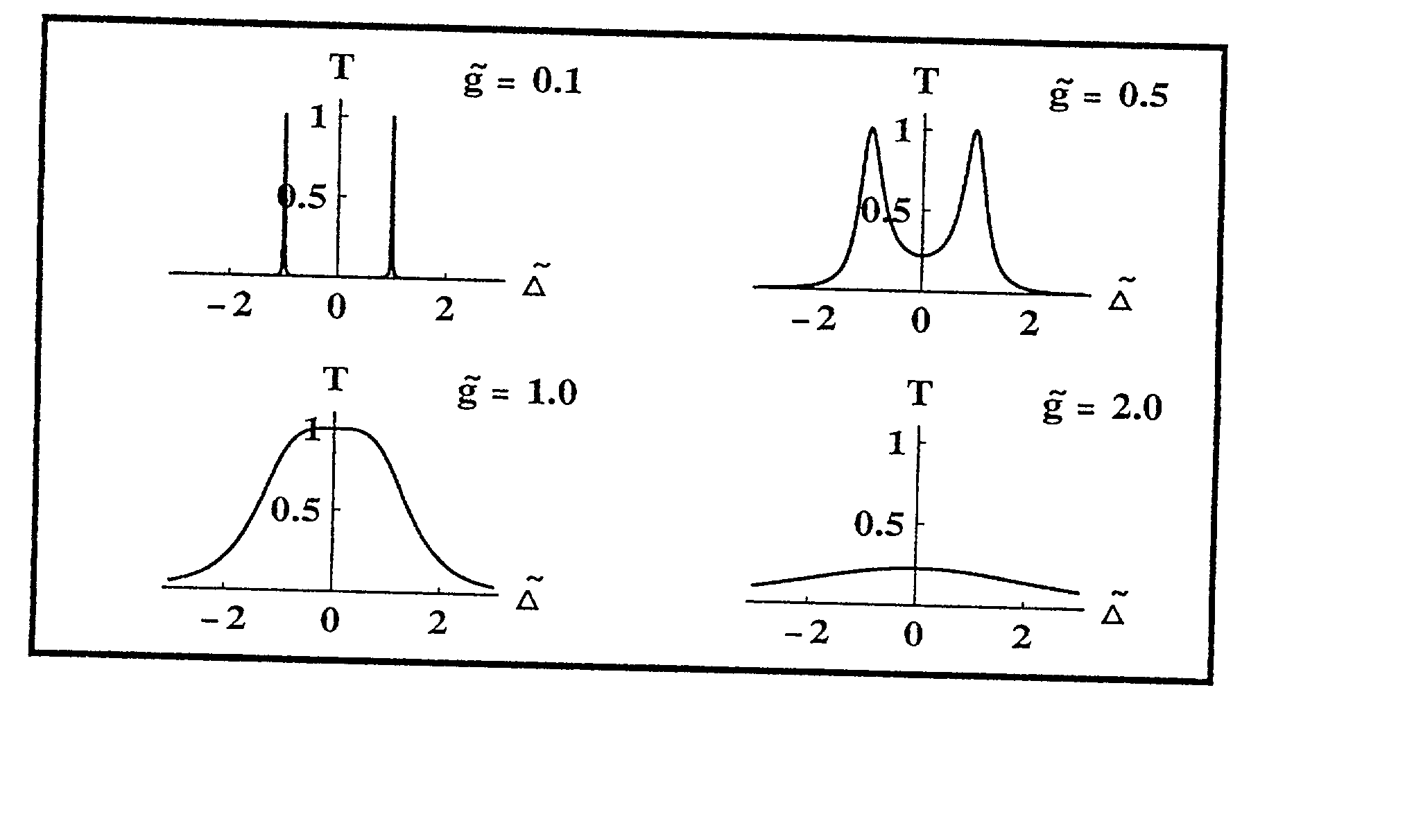
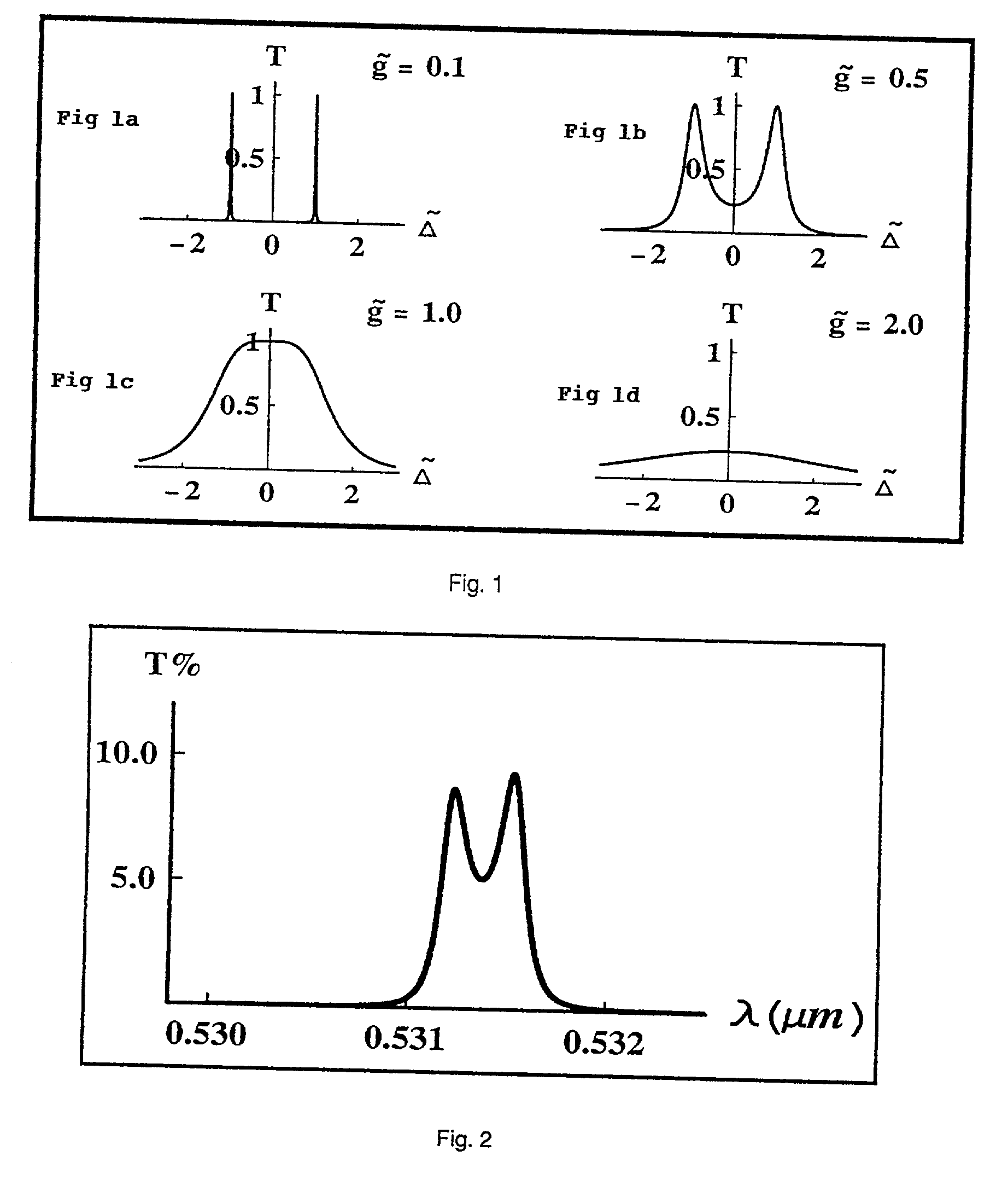
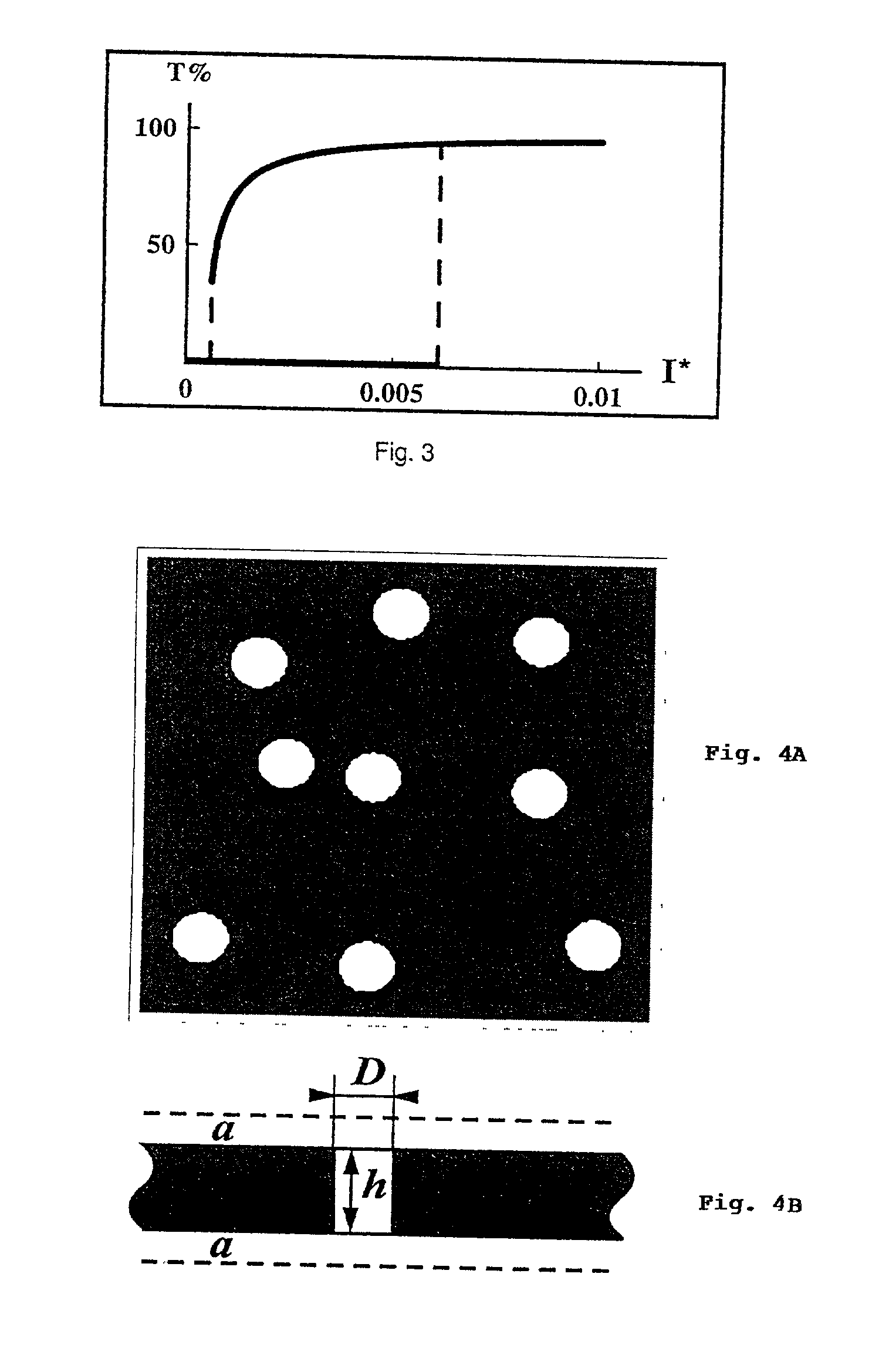
[0053] The present invention is of apparatuses and methods employing extraordinary light transmittance through an optically thick metal film with (or without) subwavelength holes. The invention is also of apparatuses, materials, and methods employing metal nanowires for enhanced spectroscopy and left-handed materials.

[0054] When subwavelength holes are employed, film transmittance has sharp peaks that are due to the Maxwell-Garnet resonances in such holes. There are electric and magnetic resonances resulting in, respectively, dramatically enhanced electric and magnetic fields in the holes. An analytical expression for the resonance transmittance is stated that holds for arbitrary hole distribution in a device according to the invention. There are also other types of transmittance resonances in the case when the holes are arranged into a regular lattice. These resonances occur because of the excitation of surface plasmon polaritons propagating over the film surface. A combination of...


PUM

PropertyMeasurementUnit
lengthaaaaaaaaaa
lengthaaaaaaaaaa
light wavelengthsaaaaaaaaaa

Abstract

Controlling, guiding, manipulating, and circuiting light and performing surface-enhanced spectroscopy in a medium comprising plasmonic nanomaterials via the excitation of plasmon modes in the materials. The plasmonic nanomaterials are based on metal films with or without arrays of nanoholes and / or on metal nanowires and / or spheroids. Also devices and methods employing such plasmonic nanomaterials.

Description

[0001] This application claims the benefit of the filing of U.S. Provisional Patent Application Serial No. 60 / 286,437, entitled "Light-Controlled Extraordinary Optical Transmittance and Its Applications", filed on Apr. 25, 2001, and of the filing of U.S. Provisional Patent Application Serial No. 60 / 330,059, entitled "Resonance Transmittance Through Metal Film with Subwavelength Holes", filed on Oct. 16, 2001, and the specifications thereof are incorporated herein by reference.[0002] 1. Field of the Invention (Technical Field)[0003] The present invention relates to methods and apparatuses employing plasmonic materials for extraordinary light transmittance through optically thick metal films and other ways to control light, particularly for use in optical devices.[0004] 2. Background Art[0005] Note that the following discussion refers to a number of publications by author(s) and year of publication, and that due to recent publication dates certain publications are not to be considered...

Claims


Application Information

Patent Timeline
Patent Type & Authority Applications(United States)
IPC IPC(8): G01N21/35G01N21/55G02F1/19G02F1/35G02F3/00
CPCB82Y20/00G01N21/554G01N2021/3568G02B1/007G02F1/195G02F1/3515G02F3/00G02F2202/36G02F2203/10
Inventor SARYCHEV, ANDREY K.SHALAEV, VLADIMIR M.DYKHNE, ALEXANDER M.PODOLSKIY, VIKTOR A.
Owner NEW MEXICO STATE UNIV TECH TRANSFER
Why Eureka
Try Eureka