Fabrication method of semiconductor

Inactive Publication Date: 2003-03-27
ORIENT SEMICON ELECTRONICS
View PDF5 Cites 1 Cited by
  • Summary
  • Abstract
  • Description
  • Claims
  • Application Information

AI Technical Summary

Problems solved by technology

Due to the fact that the fabrication of IC metallic lead frame 1' requires high precision punching molds and high precision fabrication tool; the cost of packaging fabrication is high. FIG. 2 shows a sectional view of a wire-bonding package of a conventional metallic lead frame.
After the completion of the general

Method used


Image

  • Fabrication method of semiconductor
  • Fabrication method of semiconductor
  • Fabrication method of semiconductor

Examples


Embodiment Construction

[0018] For the purpose of promoting an understanding of the principles of the invention, reference will now be made to the embodiment illustrated in the drawings. Specific language will be used to describe same. It will, nevertheless, be understood that no limitation of the scope of the invention is thereby intended, alterations and further modifications in the illustrated device, and further applications of the principles of the invention as illustrated herein being contemplated as would normally occur to one skilled in the art to which the invention relates.

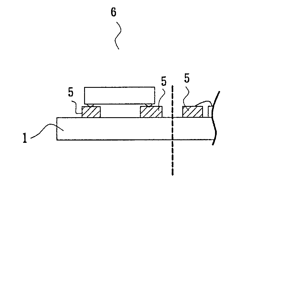
[0019] FIGS. 4A to 4G show a fabrication method of semiconductor packaging and the packaging element, wherein a heat-resistant tape is used as substrate and the surface of the substrate is formed into circuit layout. After electrically bonding with chip, a packaging is formed. By removing the heat-resistant tape from the chip, a packaging element is obtained.

[0020] In accordance with the present invention, the fabrication of ch...


PUM


Abstract

A fabrication method of semiconductor packaging and the packaging element is disclosed. A layer of copper is formed on a thick heat-resistant tape and the surface of the copper layer is coated with a light sensitive photoresist. A light source passes through a pre-fabricated circuit negative being performed on the copper layer such that the photoresist is retained on the surface of the copper layer. An etching step is performed so as to obtain a copper wire with circuit diagram. After that, a wire bonding or a flip chip method is used to bind copper wire circuit with the chip. An appropriate packaging method is performed, a packaging element is obtained after the heat-resistant tape is removed.

Description

[0001] (a) Field of the Invention[0002] The present invention relates semiconductor packaging, and in particular, a method of fabrication of packaging element.[0003] (b) Description of the Prior Art[0004] Conventional type of packaging method in obtaining thin size packaging is by means of metallic lead frame. As shown in FIG. 1, there is shown a top view of a metallic lead frame 1'. Due to the fact that the fabrication of IC metallic lead frame 1' requires high precision punching molds and high precision fabrication tool; the cost of packaging fabrication is high. FIG. 2 shows a sectional view of a wire-bonding package of a conventional metallic lead frame.[0005] In conventional semiconductor packaging, the chips are adhered onto the metallic lead frame'. After that gold wire 3' is used to connect an aluminum pad 22' of the chip 2' and the lead connection pin 13' of the metallic lead frame 1'. In packaging by employing metallic lead frame 1', a chip carrier board is needed so as to...

Claims


Application Information

Patent Timeline
IPC IPC(8): H01L25/18H01L21/68H01L23/52H01L23/538H01L25/065H01L25/10H01L25/11
CPCH01L21/6835H01L23/5387H01L24/45H01L25/0657H01L25/105H01L2224/16H01L2224/32145H01L2224/45147H01L2224/48225H01L2224/73204H01L2224/73265H01L2225/06517H01L2225/0652H01L2225/06568H01L2225/06579H01L2225/06582H01L2225/06586H01L2924/01004H01L2924/01039H01L2924/0105H01L2924/01079H01L2924/14H01L2924/15311H01L2924/00014H01L24/48H01L2224/32225H01L2224/45144H01L2924/00H01L2225/1023H01L2225/107H01L2924/01013H01L2924/01028H01L2224/48227H01L2924/181H01L2924/00012
Inventor SHIEH, WEN-LOHUANG, NINGCHEN, HUI-PINCHIANG, HUA-WENCHANG, CHUNG-MINGTU, FENG-CHANGHUANG, FU-YUCHANG, HSUAN-JUIHU, CHIA-CHIEHLEU, WEN-LONG
Owner ORIENT SEMICON ELECTRONICS
Why Eureka
Try Eureka