Spacers for field emission displays

a technology for field emission displays and spacers, which is applied in the manufacture of electric discharge tubes/lamps, tubes with screens, discharge tubes luminescnet screens, etc., can solve the problems of not having the structural strength for forming spacers in feds, polyimide is not an ideal material for photosensitive use, and polyimide is not ideal for use as a spacer

Inactive Publication Date: 2003-05-08
MICRON TECH INC
View PDF5 Cites 55 Cited by
  • Summary
  • Abstract
  • Description
  • Claims
  • Application Information

AI Technical Summary

Benefits of technology

0012] These and other objects are provided by an improved method for forming spacers in an FED. In one aspect of the invention, the method uses photoresist as a

Problems solved by technology

However, as will be discussed below, the spacers disclosed by the '327 patent are not ideal and there remains a need for improved spacers and for methods of making such improved spacers.
For example, polyimide is not an ideal photosensitive material.
Also, polyimide is not an ideal material for use as a spacer in an FED.
Renaud, Institute

Method used


Image

  • Spacers for field emission displays
  • Spacers for field emission displays
  • Spacers for field emission displays

Examples


Embodiment Construction

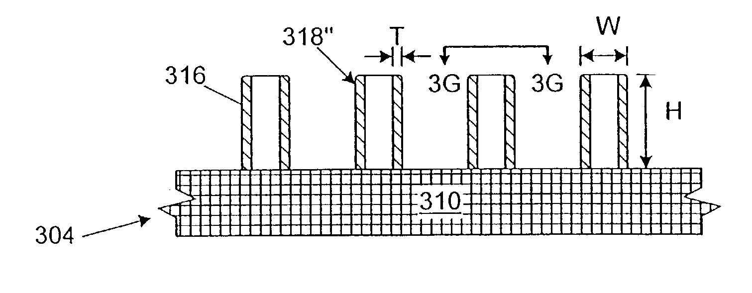
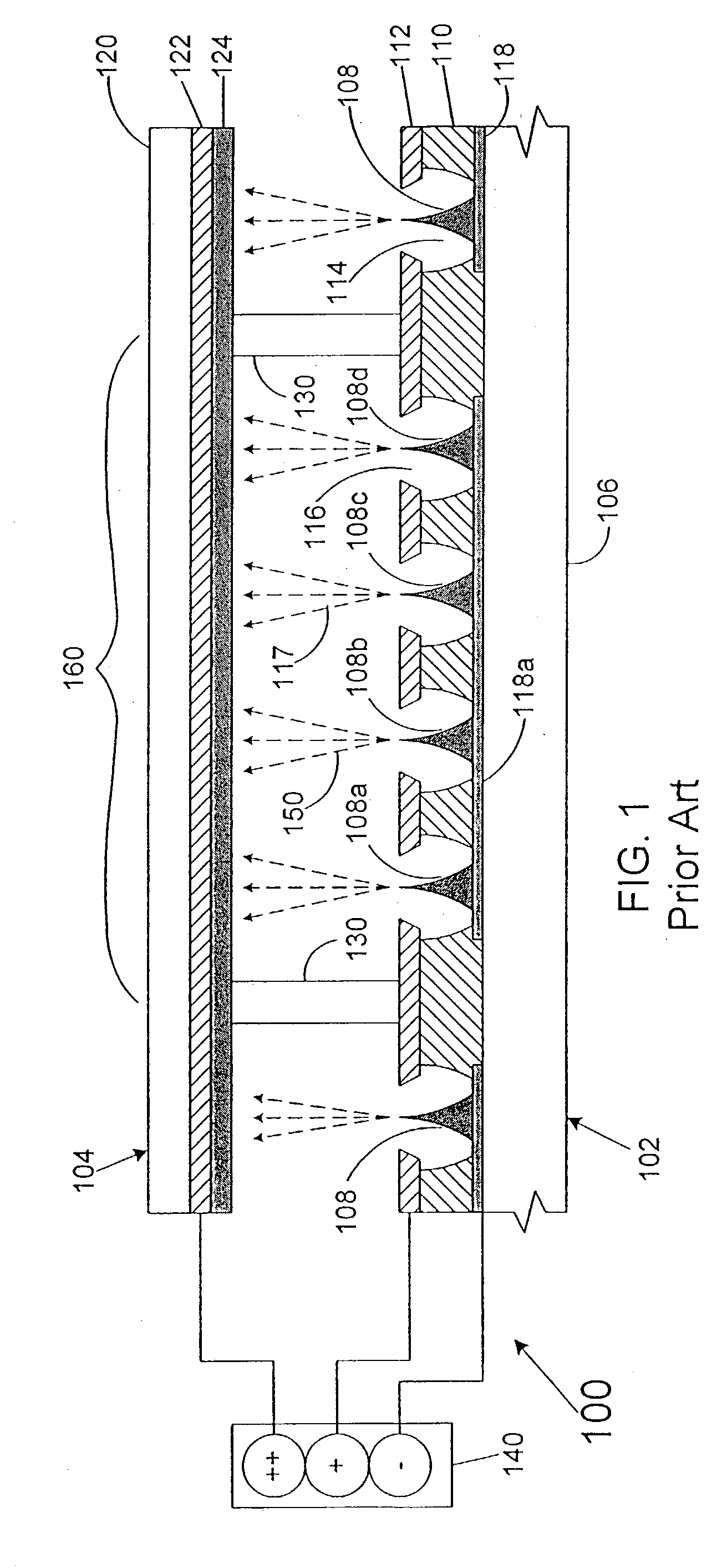
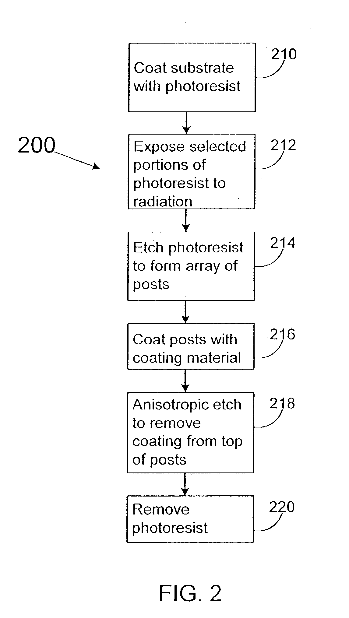
[0025] FIG. 2 shows a flow chart of a method 200 according to the invention for constructing improved spacers for use in FEDs. FIGS. 3A-3G illustrate examples of the structures formed according to the invention at various steps of the method 200. Step 210 is the first step in method 200 and FIG. 3A shows the structure 300 formed after completion of step 210. The structure 300 includes a substrate 310 and a layer of photoresist 312 that is formed over the substrate 310. The layer of photoresist 312 preferably comprises a layer of SU-8 type photoresist. As will become clearer from the description below, the photoresist 312 is used to form spacers in a FED. Although the substrate 310 could comprise any surface, the substrate 310 typically comprises the baseplate of an FED (e.g., such as baseplate 102 as shown in FIG. 1). Further, the upper portion of the substrate 310 that contacts the photoresist 312 could comprise the grid layer of the FED's baseplate (e.g., such as grid layer 112 as...


PUM


Abstract

The disclosed method for forming a field emission display includes forming a cathode and an anode, forming a plurality of photoresist posts over the cathode, and coating the posts with a coating material. The coating material forms sidewalls around the posts. The photoresist posts may then be removed from within the sidewalls. The anode may then be fitted onto the sidewalls so that the sidewalls function as spacers in the field emission display.

Description

BACKGROUND OF THE INVENTION[0002] The present invention relates to improved spacers for use with field emission displays (FEDs). U.S. Pat. No. 5,063,327 discloses a prior art method of fabricating spacers for use in FEDs. However, as will be discussed below, the spacers disclosed by the '327 patent are not ideal and there remains a need for improved spacers and for methods of making such improved spacers.[0003] Prior to discussing spacers, the general background of FEDs will be briefly reviewed. FIG. 1 shows a cross sectional view of a portion of a prior art FED 100. FED 100 includes a cathode, or baseplate, 102 and an anode, or faceplate, 104. Baseplate 102 includes a substrate 106, a plurality of field emitters 108, an insulating layer 110, and a conductive grid layer 112. Insulating layer 110 is disposed over substrate 106, and grid layer 112 is disposed over insulating layer 110. Insulating layer 110 defines a plurality of void regions 114, and each emitter 108 is disposed over ...

Claims


Application Information

Patent Timeline
IPC IPC(8): H01J9/18H01J9/24H01J29/02H01J29/86H01J31/12
CPCH01J9/18H01J9/185H01J9/242H01J29/028H01J29/864H01J31/123H01J2329/864H01J2329/8645
Inventor CATHEY, DAVID A.ALWAN, JAMES J.
Owner MICRON TECH INC
Why Eureka
Try Eureka