Inductively coupled plasma source for improved process uniformity

a plasma source and inductive coupling technology, applied in the direction of electrical equipment, basic electric elements, electric discharge tubes, etc., can solve the problems of increasing complexity, high aspect ratio, and increasing the requirement for improved design features resolution, and achieving the effect of improving process uniformity, reducing manufacturing costs, and reducing manufacturing costs

Inactive Publication Date: 2003-05-08
TOKYO ELECTRON LTD
View PDF12 Cites 120 Cited by
  • Summary
  • Abstract
  • Description
  • Claims
  • Application Information

AI Technical Summary

Problems solved by technology

Increasing miniaturization of technology increases the demand for improved resolution in design features with increasing complexity and higher aspect ratios.
In spite of significant advances, most etch processes still induce a non-uniform and undesirable etch profile.
Non-uniformity can be caused by a non-symmetrical exhaust flow, temperature variations, non-uniform plasma chemistry, non-uniform ion density or non-uniform gas supply.
In addition, conventional plasma processing devices utilize plasma sources comprising a significant number of complex components leading to excessive fabrication times, fabrication costs and problems with the consistency of the plasma source assembly.
Furthermore, maintaining a semiconductor-processing machine is time consuming and an expensive procedure.
Removing and servicing parts above the wafer that produce plasma cause machine downtimes that add to the overall cost to process each wafer.
Conventional plasma processing devices are not amenable to quick and efficient maintenance and service of plasma sources and, therefore, machine down-time can be significant.

Method used


Image

  • Inductively coupled plasma source for improved process uniformity
  • Inductively coupled plasma source for improved process uniformity
  • Inductively coupled plasma source for improved process uniformity

Examples


second embodiment

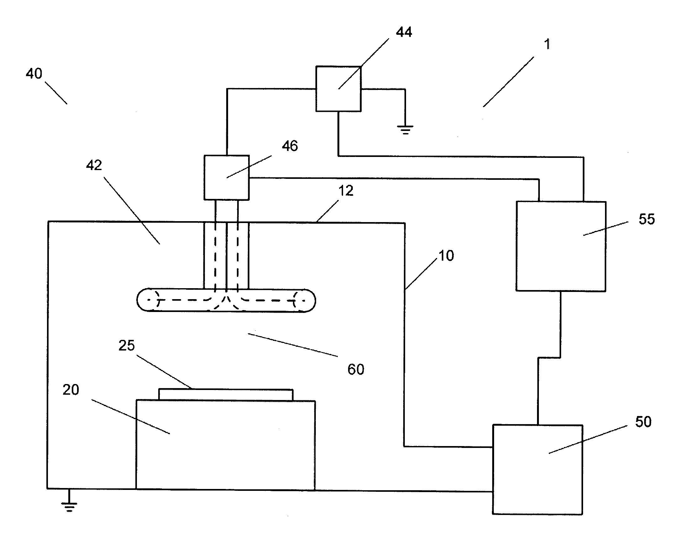
[0041] Referring now to FIG. 6, the present invention is shown. A plasma processing system comprises a chamber 110 and a plasma source 140, wherein plasma source 140 further includes a plurality of inductive coil assemblies 142A, 142B and 142C. RF power is coupled to each inductive coil assembly 142(A-C) via RF generators 144 (A-C) through respective impedance match networks 146 (A-C). A controller 155 is coupled to each RF generator 142 (A-C), each impedance match network 146 (A-C) and vacuum pumping system 150. The inductive coil assemblies 142A, 142B and 142C are arranged within the process chamber 110 and can extend to different distances from upper wall 112 of chamber 110 into plasma region 160 as shown in FIG. 6, or they can extend to the same distance from upper wall 112. A plurality of inductive coil assemblies 142 (A-C), as exemplified in FIG. 6, can enable adjustment of the plasma uniformity local to substrate 25. The coils include concentric shapes (e.g., rings) that are ...

third embodiment

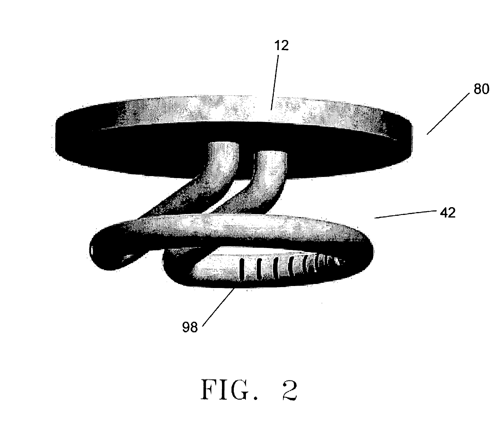
[0042] Referring now to FIGS. 7A (side view) and 7B (top view), the present invention is shown. A plasma processing system 200 comprises a chamber 210 and a plasma source 240, wherein plasma source 240 further includes a linear inductive coil assembly 242. RF power is coupled to linear inductive coil assembly 242 via RF generator 244 through an impedance match network 246. The linear inductive coil assembly 242 is arranged within the process chamber 210 and can be positioned a finite distance below upper wall 212 of chamber 210 above substrate 25 as shown in FIG. 7A. Furthermore, the linear inductive coil assembly 242 can extend across chamber 210 in a transverse direction making several passes above substrate 25 (25') as shown in FIG. 7B. For example, in FIG. 7B, four (4) passes across chamber 210 are made with inductive coil assembly 242. The linear inductive coil assembly 242 further comprises an inner conductor 290 surrounded by a slotted outer conductor 292, between which is in...


PUM


Abstract

An improved apparatus for material processing, wherein the improved apparatus including a plasma processing system to process a substrate, the plasma processing system including a process chamber, a substrate holder, and a plasma source. The plasma source further includes an inductive coil assembly for inductively coupling RF power to plasma wherein the inductive coil assembly is arranged within a process chamber. The inductive coil assembly includes an inner conductor, a slotted outer conductor, and a dielectric layer. The inductive coil assembly can further include a second dielectric layer in order to protect the slotted outer conductor from plasma. The inner conductor is surrounded by the slotted outer conductor and, between which, resides the first dielectric layer. The second dielectric layer encapsulates the inner conductor, first dielectric layer and the slotted outer conductor.

Description

[0001] This application claims priority to United States provisional serial no. 60 / 331,033, filed on Nov. 7, 2001, the entire contents of which are herein incorporated by reference.[0002] 1. Field of Invention[0003] The present invention relates to inductively coupled plasma sources and more particularly to inductively coupled plasma sources for improved process uniformity.[0004] 2. Description of Related Art[0005] Plasma processing systems are used in the manufacture and processing of semiconductors, integrated circuits, displays and other devices or materials, to both remove material from or to deposit material on a substrate such as a semiconductor substrate.[0006] Increasing miniaturization of technology increases the demand for improved resolution in design features with increasing complexity and higher aspect ratios. In order to achieve these, improved process uniformity can be beneficial. In plasma processing systems, one factor affecting the degree of etch or deposition unif...

Claims


Application Information

Patent Timeline
Patent Type & Authority Applications(United States)
IPC IPC(8): H01J37/32H01L21/8238
CPCH01J37/321
Inventor FINK, STEVEN T.SOSNOWSKI, JANUSZ
Owner TOKYO ELECTRON LTD
Why Eureka
Try Eureka