Apparatus for assembling integrated circuit packages

a technology for assembling integrated circuits and components, applied in the direction of transportation and packaging, conveying, manufacturing tools, etc., can solve the problems of inability to optimize automation advantages, island separation of similar equipment from one another, and process, such as wire bonding, typically take a longer time than other processes, so as to improve the management of material flow.

Inactive Publication Date: 2003-05-29
ASM TECH SINGAPORE PTE LTD
View PDF0 Cites 7 Cited by
  • Summary
  • Abstract
  • Description
  • Claims
  • Application Information

AI Technical Summary

Benefits of technology

0007] It is thus an object of the present invention to provide an improved apparatus that can improve the management of the flow of materials in production line.

Problems solved by technology

This practice resulted in islands of similar equipment separated from one another.
Thus, there is a need for large buffering between the processes through the use of leadframe magazines, and manual material handling and tracking, This is inefficient, and requires special maintenance staff and a number of skilled operators to operate each stand-alone machine.
However, although the multi-station apparatus described therein reduces the need for manual transfer of leadframes during the assembly process, it fails to optimize the advantages of automation, For example, the resulting apparatus does not cater to the fact that certain processes, such as wire-bonding, typically take a longer time than other processes, such as molding.
In the event, bottlenecks are caused because a process further down the production line has to wait whilst an earlier process is being performed.
Since the machines in the aforesaid patent are quite rigidly integrated in their implementation, it will also be more difficult to change machines in the production line with minimal modifications to the apparatus as a whole.

Method used


Image

  • Apparatus for assembling integrated circuit packages
  • Apparatus for assembling integrated circuit packages
  • Apparatus for assembling integrated circuit packages

Examples


Embodiment Construction

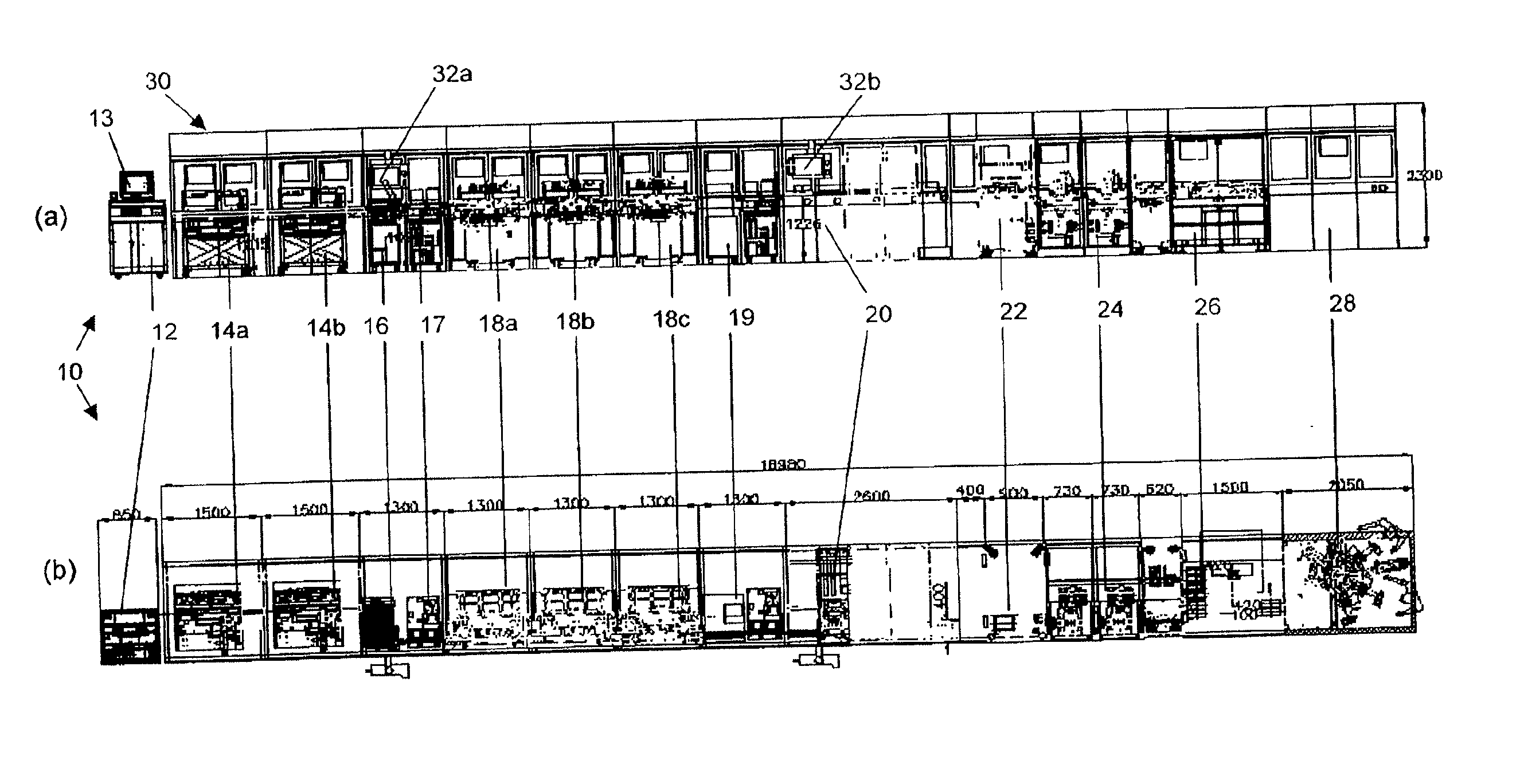
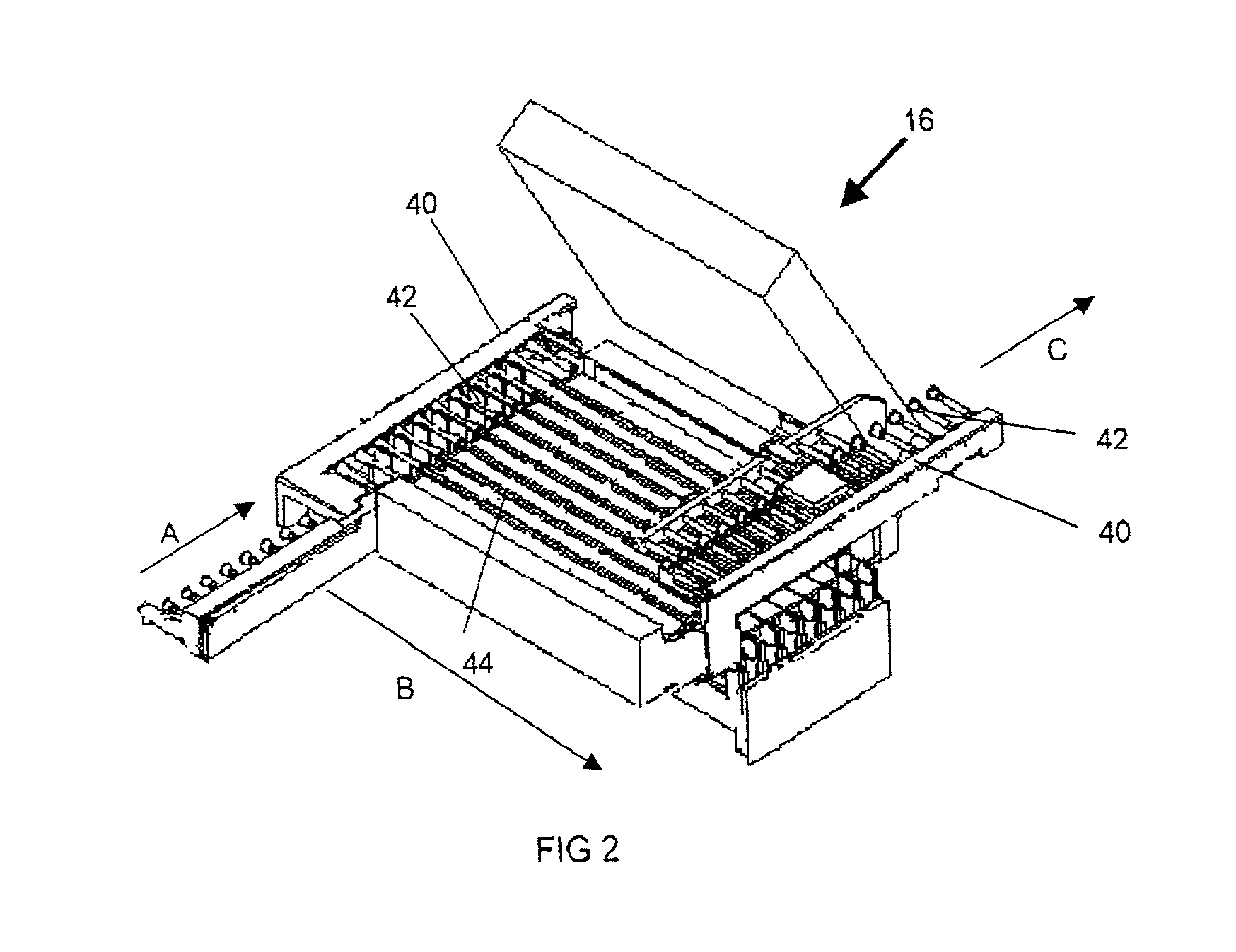
[0018] FIG. 1 at 1(a) and 1(b) illustrates a front elevation and a plan view respectively of an IC assembly apparatus according to a preferred embodiment of the invention. The illustrations show a cell controller 12 that includes a microprocessor, and display screen 13 to monitor and control the processes taking place in the production line constituting the apparatus 10 for processing materials, for example, to produce a semiconductor leadframe package. The cell controller 12 can be positioned anywhere, although in this embodiment, it is positioned adjacent to the production line. The first machine in the apparatus 10 is a die-bonder 14a, 14b to place and bind a die to a semiconductor leadframe (not shown). After die-bonding, the die and leadframe are cured in a cure oven 16 and then enter an input buffer 17.

[0019] The input buffer 17 controls the entry of leadframes to wire bonders 18a, 18b, 18c. The leadframes then enter into an output buffer position 19, to control the entry of l...


PUM

PropertyMeasurementUnit
displacementaaaaaaaaaa
heightaaaaaaaaaa
distanceaaaaaaaaaa

Abstract

The invention relates to an apparatus (10) for the manufacture of a component such as an integrated circuit chip, including: a plurality of processing stations (14a, 14b, 16, 18a, 18b, 18c, 19, 20, 22, 24, 26, 28) forming a production line for the manufacture of said component: conveying means (42) adapted to transport component forming materials from one processing station to another in the production line; and storage means (17) of the production line for storing said materials during transport along the production line. The storage means (17) acts as buffers effectively to collect materials and store them for efficient transport along the production line.

Description

[0001] The present invention relates to an apparatus used for the assembly of a semiconductor device such as an Integrated circuit ("IC") package, and in particular to an apparatus that automates the assembly process.BACKGROUND AND PRIOR ART[0002] Typically, the manufacture of an IC package from the raw-material stage to the finished product involves a plurality of processes. In the case of leadframe packages, semiconductor die is first bonded to a leadframe by a bonding agent. Thereafter, the leadframe is heated in a curing oven to strengthen the bond between the die and the leadframe. The bonding pads of the die and the load frame are then bonded to each other for conductivity by means of wire-bonding, commonly using gold or copper wires. The die is thereafter encapsulated with a resin material, which is molded over the die and leadframe. The resin material is then cured by heating before each encapsulated die is singulated from the other dies in the leadframe by a so-called trim-...

Claims


Application Information

Patent Timeline
Patent Type & Authority Applications(United States)
IPC IPC(8): H01L21/00
CPCH01L21/67236Y10T29/53413Y10T29/49144Y10T29/49128Y10T29/53409Y10T29/53365Y10T29/53187Y10T29/53174Y10T29/5313
Inventor HOW, WEE KIUNZHANG, JIANTAN, LIAN HOK
Owner ASM TECH SINGAPORE PTE LTD
Why Eureka
Try Eureka