Method and system for quantifying the step profile characteristics semiconductor features using surface analysis data

a technology of surface analysis and semiconductor features, applied in the field of electronic chip tools, can solve the problems of inability to fully characterize the process step, inability to quantify the edge profile of any given feature, and inability to achieve the full characterization of the process step

Inactive Publication Date: 2003-06-12
IBM CORP
View PDF13 Cites 10 Cited by
  • Summary
  • Abstract
  • Description
  • Claims
  • Application Information

AI Technical Summary

Problems solved by technology

At these dimensions, characteristics of the profile of an edge of any given feature may have severe impact on further processing or more importantly the final electrical response of devices and wiring.
In-line quantitative process controls are limited by two-dimensional (top down) metrology which does not allow for full characterization of the process step.
This is an expensive and time-consuming task.
However, engineering process window definitions are generally the only application for three dimensional imaging equipment due to the slower information acquisition times. Faster two dimensional imaging equipment is then used for process controls.
However, there currently are no quantitative metrology algorithms for determining critical feature characteristics.

Method used


Image

  • Method and system for quantifying the step profile characteristics semiconductor features using surface analysis data
  • Method and system for quantifying the step profile characteristics semiconductor features using surface analysis data
  • Method and system for quantifying the step profile characteristics semiconductor features using surface analysis data

Examples


Embodiment Construction

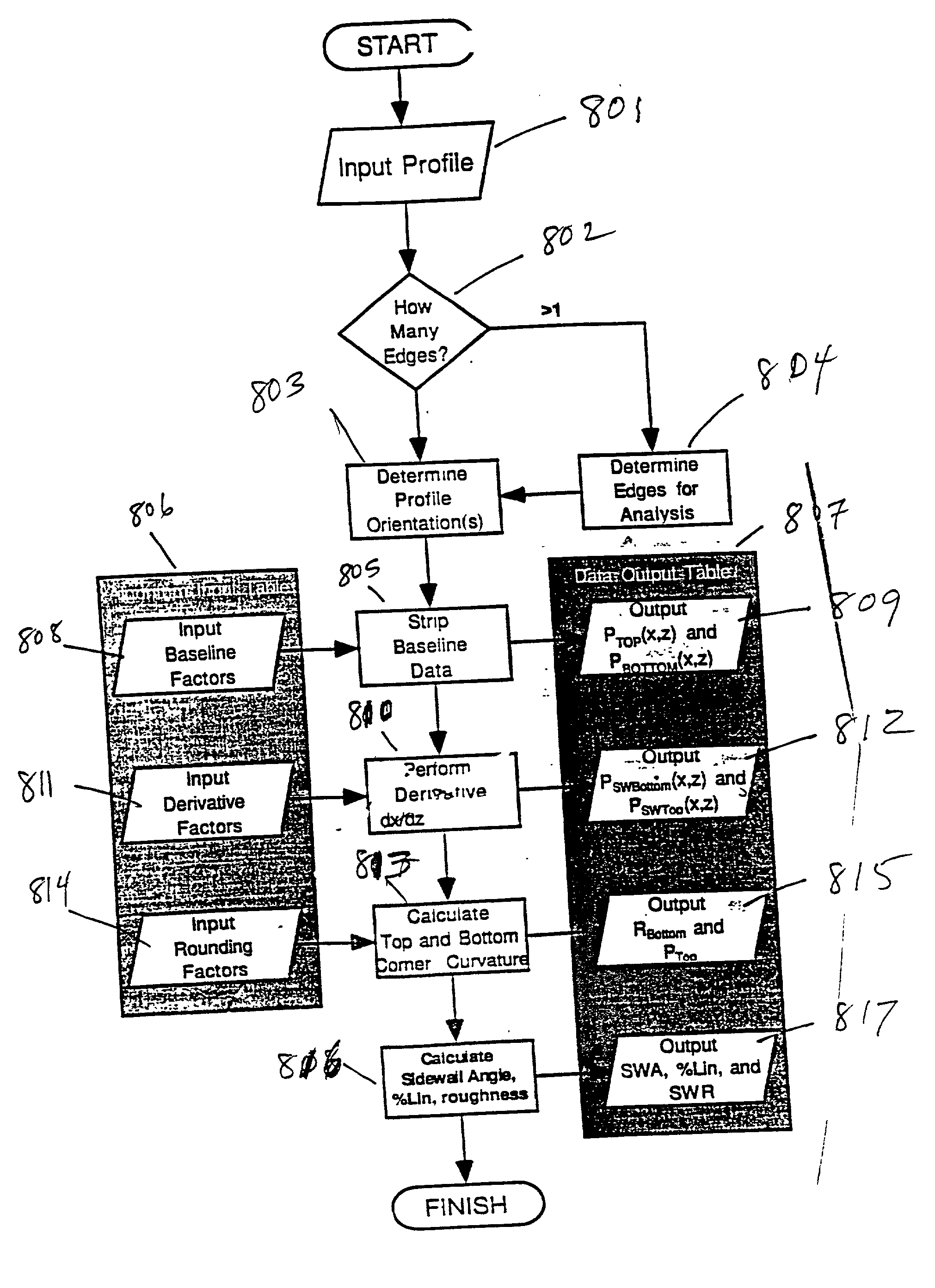
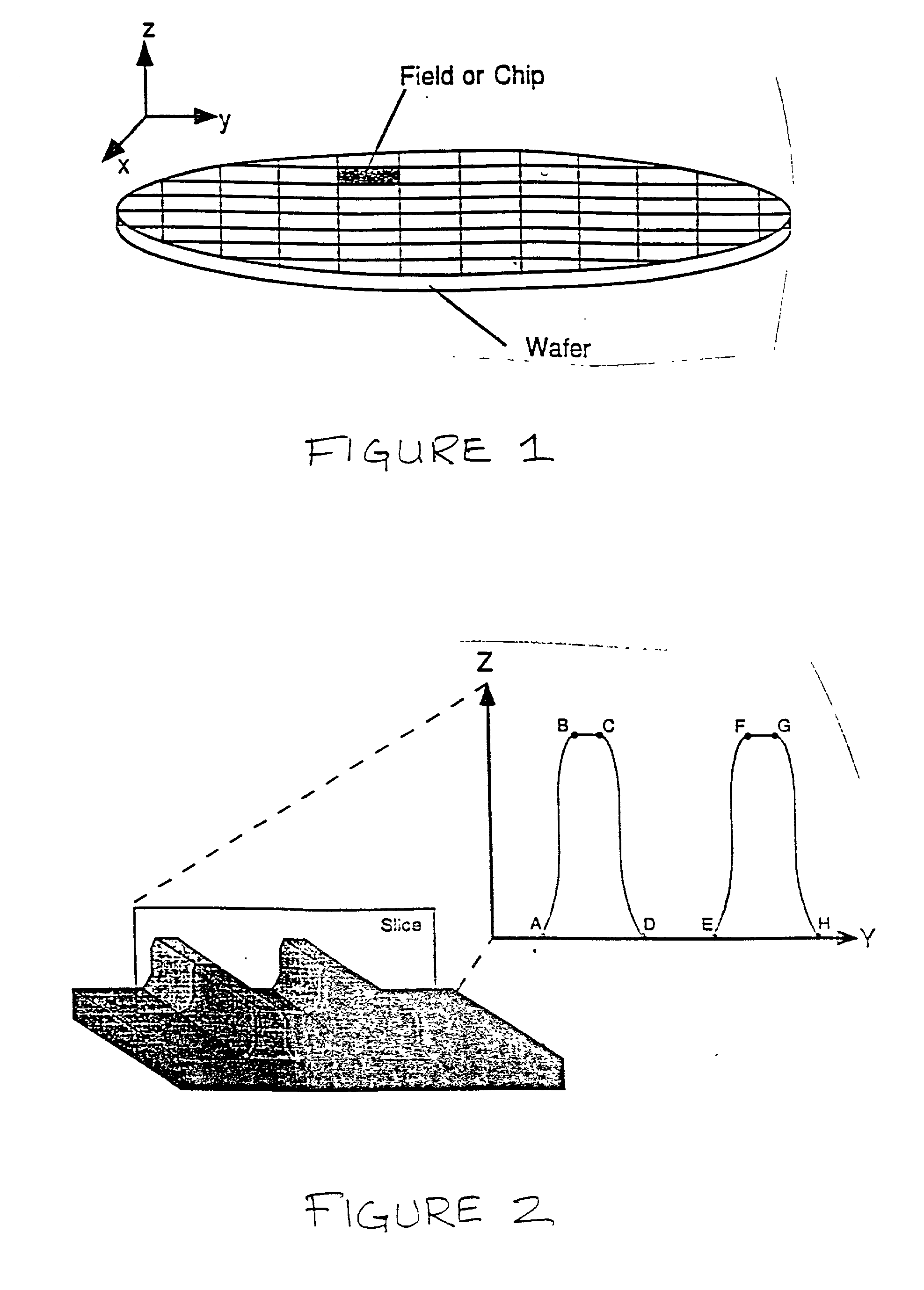
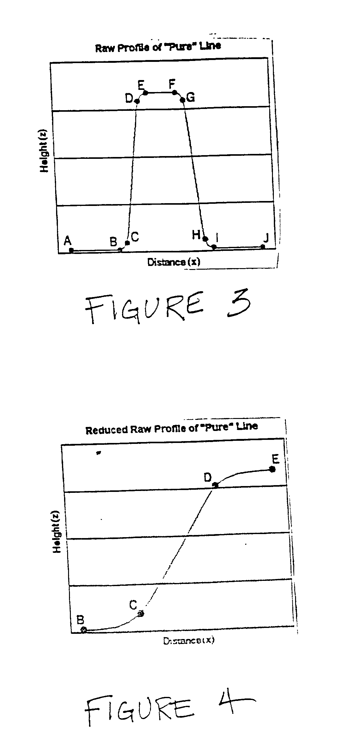
[0036] Referring now to the drawings, and more particularly to FIG. 3, an algorithm used to evaluate an LH or RH profile is described. As an example, an LH profile is quantified from a line profile, as shown in FIG. 3, by first determining what regions are the background (regions A-B and E-F) and what region is part of the edge (region B-B). The metrology equipment will generate a profile that can be assumed to comprise the region A-F from the data shown in FIG. 3. For this work, a spatial averaging technique is utilized to remove the baseline data. However, many techniques can be employed with equal success.

[0037] For example, starting at point "A" a user-defined odd number of data points are selected bounding the point. For example, if five data points are used, then two data points to the left of the data point and two data points to the right of the data point are used for the analysis. The average height of the five data points is determined. Next, the reference data point is m...


PUM


Abstract

A method and system for quantifying profile characteristics of semiconductor devices, including receiving profile data for a device under evaluation and isolating from the profile data a region indicating a profile edge. The profile edge data is rotated by ninety degrees to become rotated profile edge data. The non-rotated profile edge data or rotated profile edge data is then used to calculate at least one geometric parameter describing the profile edge.

Description

DESCRIPTION[0001] 1. Field of the Invention[0002] The present invention generally relates to tools for fabrication of electronic chips. Specifically, the technique provides for rapid quantification of critical profile characteristics for advanced semiconductor process monitoring and control.[0003] 2. Description of the Related Art[0004] Conventional semiconductor wafer processing technology is rapidly developing structures such as lines, spaces, contacts, bars, vias, etc., with dimensions less than 130 nm. The edge, or profile, structural component at these dimensional tolerances becomes a significant percentage of the overall feature. At these dimensions, characteristics of the profile of an edge of any given feature may have severe impact on further processing or more importantly the final electrical response of devices and wiring.[0005] FIG. 1 shows a typical conventional wafer with multiple chips fabricated thereon. As is well known in the art, a multitude of process steps durin...

Claims


Application Information

Patent Timeline
Patent Type & Authority Applications(United States)
IPC IPC(8): G01Q30/02G01Q30/04G01Q60/24G01Q80/00G06T5/00G06T7/00G06T7/60H01L21/00
CPCG06T7/0004G06T7/0083G06T7/602H01L21/67288G06T2207/10056G06T2207/30148G06T7/604G06T7/12G06T7/62G06T7/64
Inventor HAYES, TIMOTHY S.
Owner IBM CORP
Why Eureka
Try Eureka