Bump fabrication method

Inactive Publication Date: 2003-07-10
ADVANCED SEMICON ENG INC
View PDF0 Cites 11 Cited by
  • Summary
  • Abstract
  • Description
  • Claims
  • Application Information

AI Technical Summary

Benefits of technology

0017] In accordance with an aspect of the present invention, prior to forming the solder layer pattern, the wetting layer and the barrier layer are removed, and after a solder layer pattern is formed, only the exposed adhesion layer is removed, avoiding etching the solder layer pattern in the course of etching the solder layer and t

Problems solved by technology

When the solder layer is etched by the etching solution two problems will arise.
(1) If the etching solution etches the surface of the solder layer, the volume of the solder

Method used


Image

  • Bump fabrication method
  • Bump fabrication method
  • Bump fabrication method

Examples


Embodiment Construction

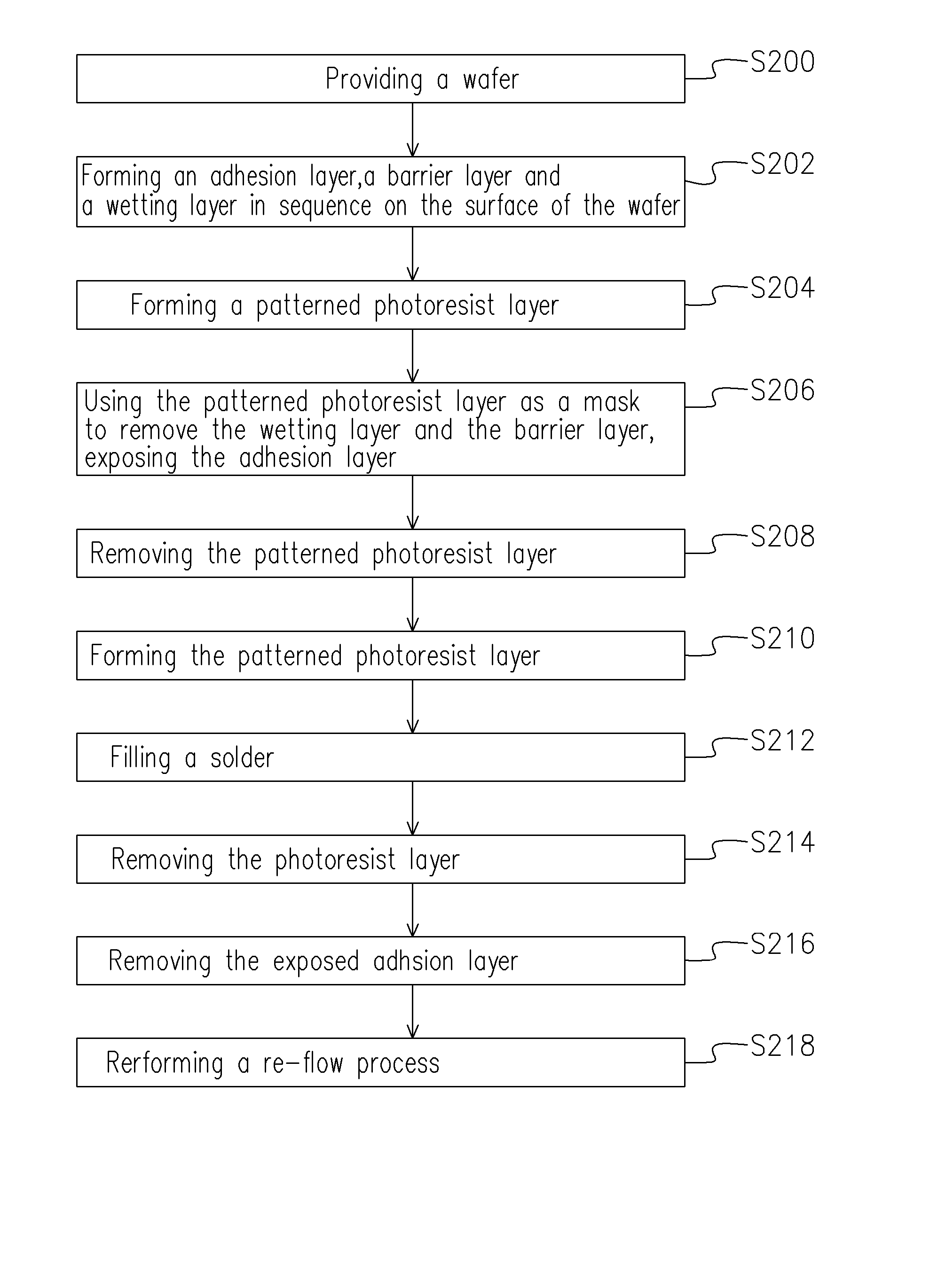
[0023] FIGS. 9 to 17, in combination with FIG. 18, show sectional views of a preferred method of fabricating bumps in accordance with the present invention. FIG. 18 is a block diagram flowchart showing a method of fabricating bumps in accordance with the present invention.

[0024] As shown in FIG. 9, the method of fabricating bumps comprises providing a wafer 200 (S200 as shown in FIG. 18) having a plurality of pads 202 and a passivation layer 204 covering the surface of the wafer 200 and exposing the pads 202, wherein the material of the passivation layer includes SiO.sub.2, SiN.sub.4, etc. Next, on the surface of the wafer 200, are formed an adhesion layer 206, a barrier layer 208 and a wetting layer 210 (S202 as shown in FIG. 18), wherein the material for the adhesion layer 206 includes Cr, Cu, Al or Ti etc., and the material for the barrier layer includes Ti-W alloy, Ti, Ni-V alloy, or Cr-Cu alloy etc. The material for the wetting layer includes Cu, Ni, Pd, Au, Ag or Pt, etc.

[0025...


PUM


Abstract

Abstract of Disclosure A method of fabricating bumps is disclosed. In the present method, prior to forming solder layer pattern, the wetting layer and the barrier layer are removed, and after a solder layer pattern is formed, only the exposed adhesion layer is removed. The method can avoide etching the solder layer pattern in the course of etching the solder layer and the barrier layer, and therefore the volume of the required solder layer pattern can be maintained. Thus, the height of the bump after the re-flow process is maintained at an appropriate range and the required bonding force between the bump and the under ball metallurgy layer pattern can be maintained so as to improve the reliability.

Description

Cross Reference to Related Applications[0001] This application claims the priority benefit of Taiwan application serial no. 91100098, filed January 07, 2002.Background of Invention[0002] Field of the Invention[0003] The present invention relates to a bump fabrication method, and in particular, a method of forming good quality bumps, avoiding etching the solder layer pattern after the exposed wetting layer, barrier layer, and adhesion layer have been removed.[0004] Description of the Related Art[0005] The so-called bump fabrication method commonly used in flip chip technology is the formation of Under Ball Metallurgy (UBM) on the external connection point on a wafer. A wafer bump is formed on the under ball metallurgy, and finally, the wafer bump is directly connected to the substrate.[0006] General UBM is used as an interface between the bump and the pad and therefore, the UBM must possess low stress, good adhesion, strong corrosive resistance and excellent wetting properties. Norma...

Claims


Application Information

Patent Timeline
IPC IPC(8): H01L21/60
CPCH01L24/11H01L2924/014H01L2224/13099H01L2924/01013H01L2924/01022H01L2924/01029H01L2924/01046H01L2924/01047H01L2924/01074H01L2924/01075H01L2924/01078H01L2924/01079H01L2924/01082H01L2924/01005H01L2924/01006H01L2924/01023H01L2924/01024H01L2924/01033H01L2224/1147H01L24/03H01L24/05H01L24/13H01L2224/05001H01L2224/05022H01L2224/05027H01L2224/0508H01L2224/05572
Inventor WENG , CHAO-FU
Owner ADVANCED SEMICON ENG INC
Why Eureka
Try Eureka