

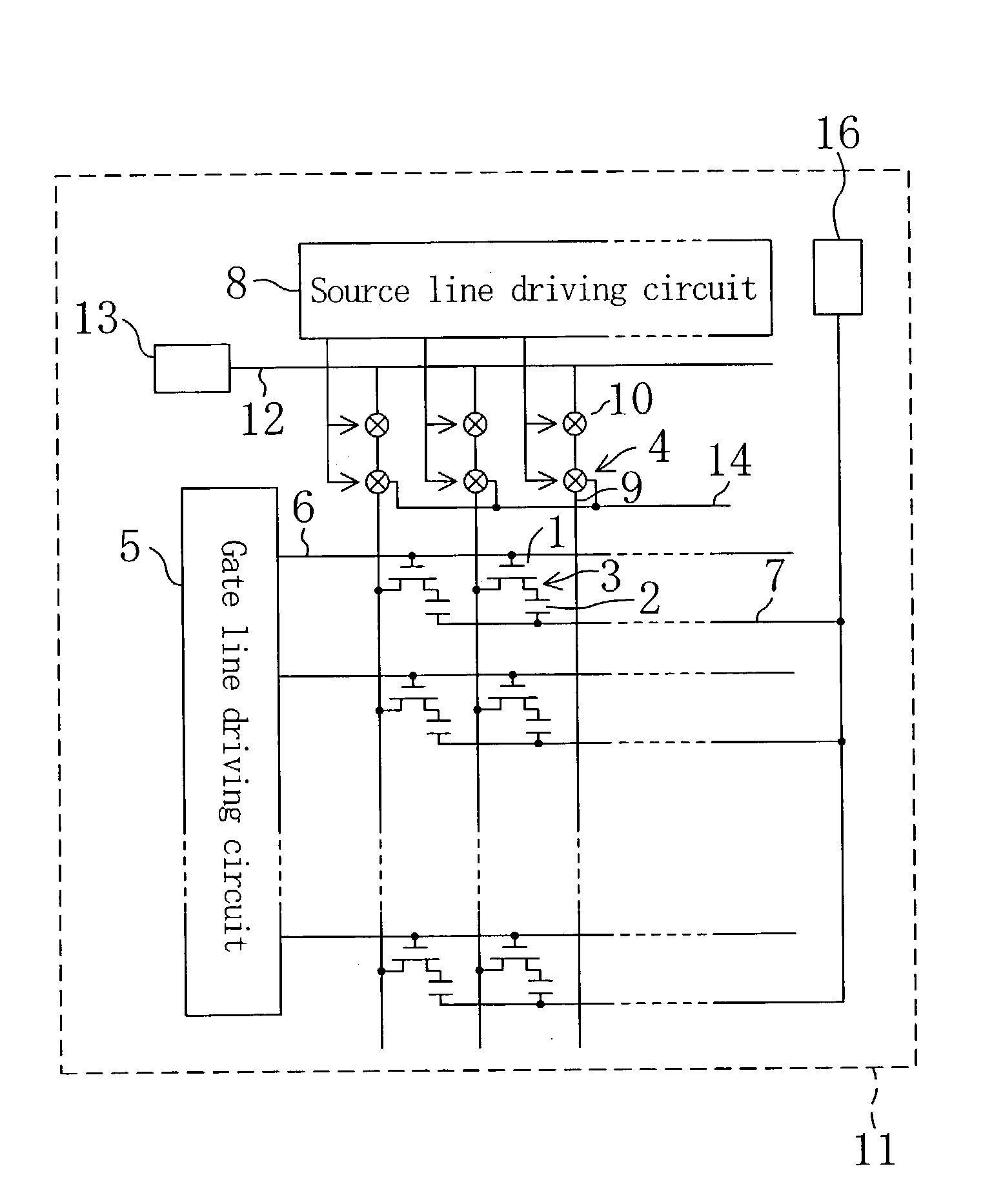
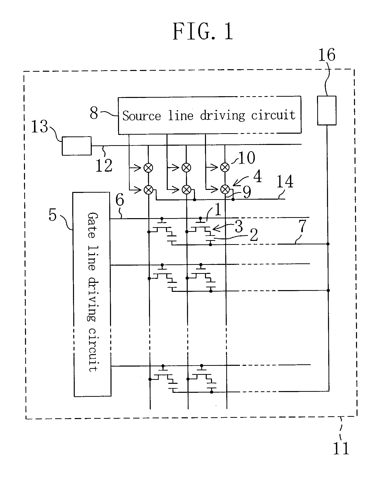
Active matrix substrate
a technology of active matrix substrate and counter substrate, which is applied in the direction of electrical testing, measurement devices, instruments, etc., can solve the problems of inability to read out data, the assembly step of attaching the active matrix substrate to the counter substrate and the liquid crystal injection step may possibly be wasted completely, and the inability to achieve high productivity
- Summary
- Abstract
- Description
- Claims
- Application Information
AI Technical Summary
Benefits of technology
Problems solved by technology
Method used
Image

Examples
embodiment 2
[0064] EMBODIMENT 2
[0065] In the present embodiment, an active matrix substrate according to the second aspect of the present invention will be described. The active matrix substrate of the present embodiment is an active matrix substrate with a built-in driving circuit, wherein the source line driving circuit is an analog driver. Note that the active matrix section is similar to that in Embodiment 1, and will not be further described below.
[0066] FIG. 4 is a block diagram illustrating an enlarged view of a portion of the active matrix substrate of the present embodiment around the source line driving circuit 8. In the active matrix substrate of the present embodiment, a number of (three) video signal lines (video lines), and a number of (three) read-out lines are provided for R, G and B pixels, respectively.
[0067] In the active matrix substrate of the present embodiment, data is first written to the storage capacitor of each picture element, and then the stored data is read out and...
embodiment 3
[0079] EMBODIMENT 3
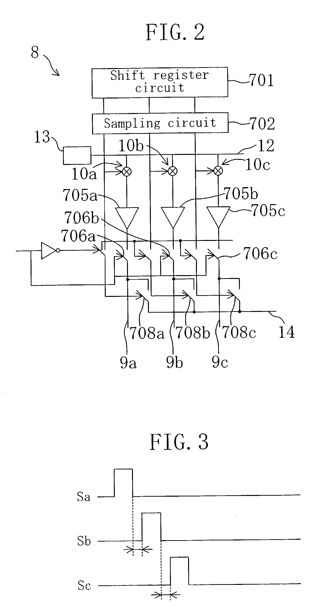
[0080] In the present embodiment, an active matrix substrate according to the first aspect of the present invention will be described. The active matrix substrate of the present embodiment is an active matrix substrate with a built-in driving circuit, wherein the source line driving circuit is a digital driver. Note that the active matrix section is similar to that in Embodiment 1, and will not be further described below.
[0081] FIG. 6 is a block diagram illustrating an enlarged view of a portion of the active matrix substrate of the present embodiment around the source line driving circuit 8. In the active matrix substrate of the present embodiment, data is first written to the storage capacitor of each picture element, and then the stored data is read out and analyzed for inspecting the active matrix substrate, as in Embodiment 1. The write operation will be described with reference to FIG. 1 and FIG. 6.
[0082] The source line driving circuit 8 includes a shift re...
embodiment 4
[0090] EMBODIMENT 4
[0091] In the present embodiment, an active matrix substrate according to the first aspect of the present invention will be described. The active matrix substrate of the present embodiment is an active matrix substrate with a built-in driving circuit, and the source line driving circuit is a digital driver, with an amplifier circuit provided at the output stage. Note that the active matrix section is similar to that in Embodiment 1, and will not be further described below.
[0092] FIG. 8 is a block diagram illustrating an enlarged view of a portion of the active matrix substrate of the present embodiment around the source line driving circuit 8. In the active matrix substrate of the present embodiment, data is first written to the storage capacitor of each picture element, and then the stored data is read out and analyzed for inspecting the active matrix substrate, as in Embodiment 1. The write operation will be described with reference to FIG. 1 and FIG. 8.
[0093] T...
PUM
| Property | Measurement | Unit |
|---|---|---|
| time | aaaaa | aaaaa |
| optical inspection | aaaaa | aaaaa |
| voltage | aaaaa | aaaaa |
Abstract
Description
Claims
Application Information