Method and structure for reducing capacitance between interconnect lines

a technology of capacitance reduction and interconnection line, which is applied in the direction of coupling contact members, basic electric elements, electrical equipment, etc., can solve the problems of increasing the difficulty of crosstalk between adjacent lines, the size of integrated circuits has continued to shrink and increase in complexity, and the interconnection spacing of integrated circuits is increasingly tigh

Inactive Publication Date: 2003-09-18
UNITED MICROELECTRONICS CORP
View PDF1 Cites 39 Cited by
  • Summary
  • Abstract
  • Description
  • Claims
  • Application Information

AI Technical Summary

Problems solved by technology

Integrated circuits have continued to shrink in size and increase in complexity with each new generation of devices.
As a result, integrated circuits increasingly require very close spacing of interconnect lines and many now require multiple levels of metalization, to interconnect the various circuits on the device.
Since closer spacing increases capacitance between adjacent lines, as the device geometries shrink and densities increase capacitance, cross talk between adjacent lines becomes more of a problem.
However, there are many issues existing in the technique of employing low K materials between tightly spaced metal lines, such as mechanical strength, dimensional stability, thermal stability, ease of pattern and etch, thermal conductivity, CMP compatibility and complexity of integration.
Many low K materials including polysilsequioxane, parylene, polyimide, benzocyclobutene and amorphous TELFLON all have the above problems, and are inferior to the currently used inter-metal dielectric material SiO.sub.2.
Thus, the low K effect of the conventional air gap is not well.

Method used


Image

  • Method and structure for reducing capacitance between interconnect lines
  • Method and structure for reducing capacitance between interconnect lines
  • Method and structure for reducing capacitance between interconnect lines

Examples


Embodiment Construction

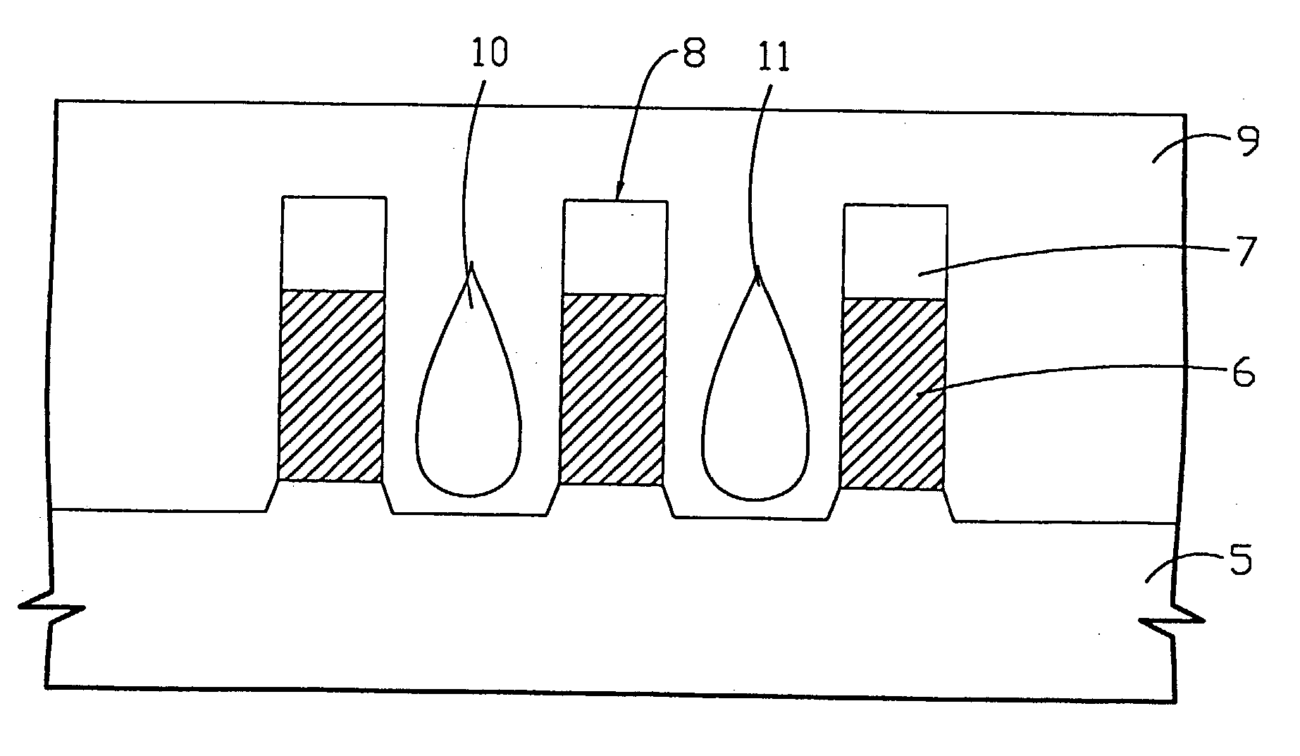
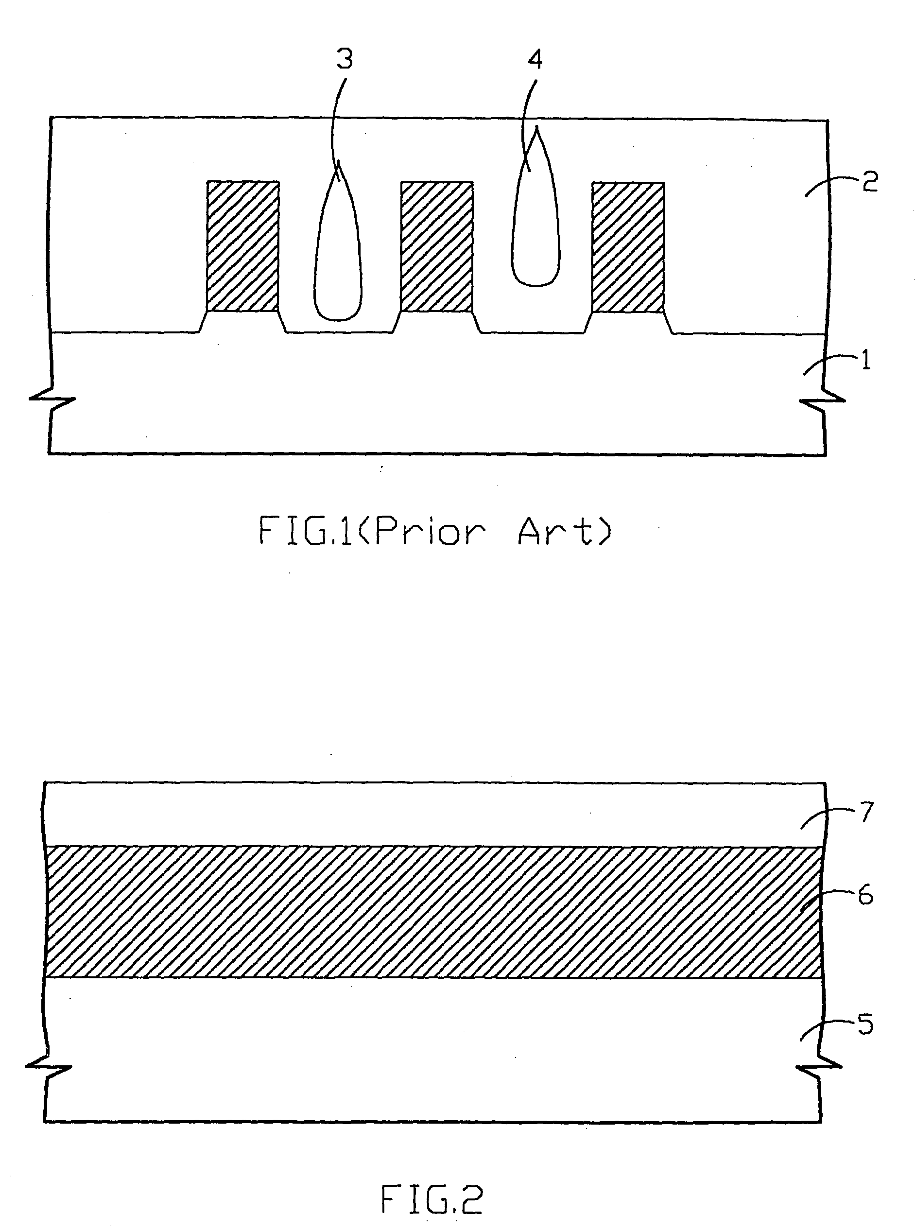
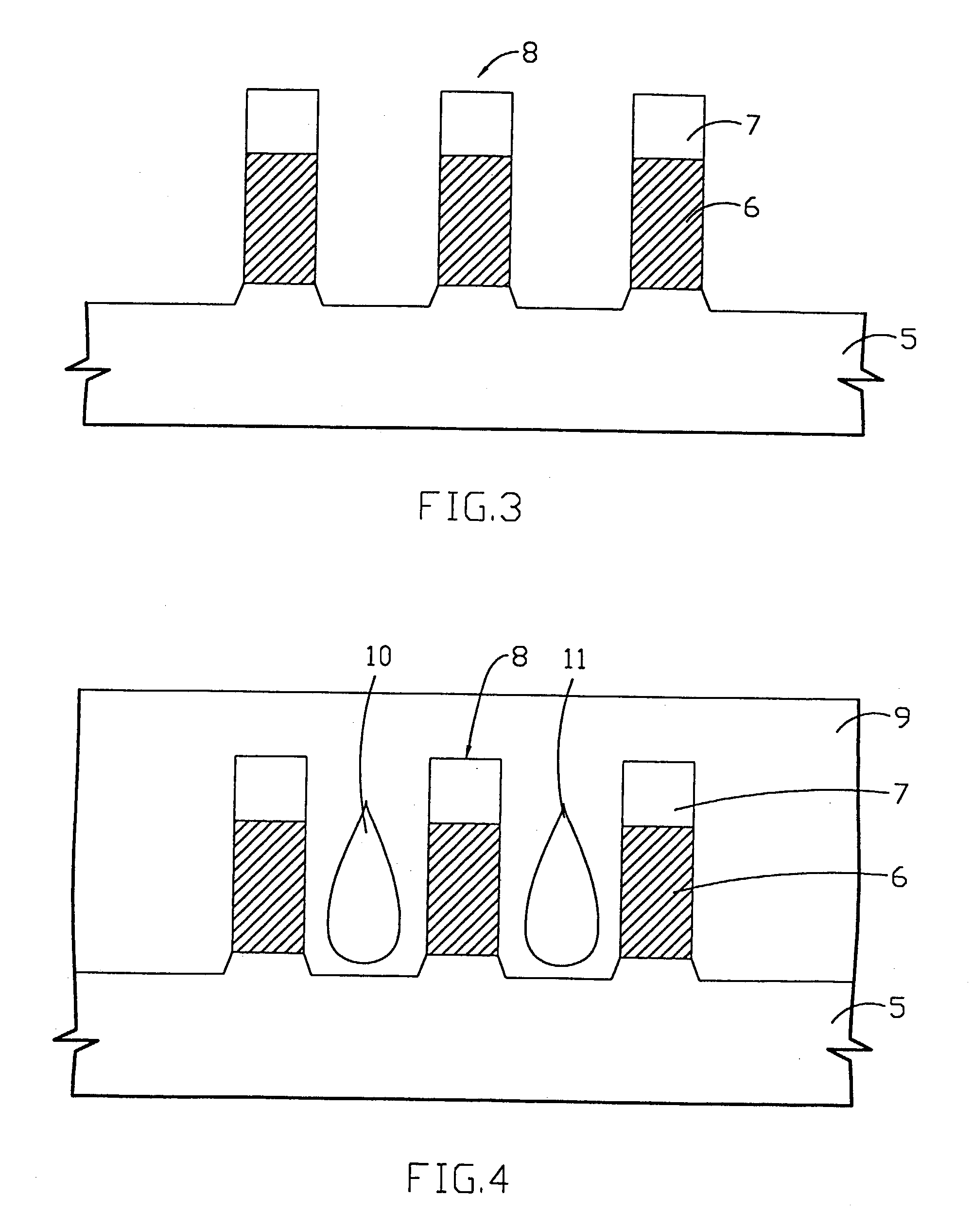
[0019] Referring to FIG. 2, the present invention firstly providing a substrate 5, having a plurality of semiconductor elements and one dielectric layer for isolating the semiconductor elements formed thereon (not shown in the figure); depositing a metal layer 6 over the substrate 5, the metal layer 6 can be an aluminum layer deposited by DC sputtering deposition method, about 3000.about.10000 angstronm thickness, the metal layer 6 also can be formed by metals selected from the group consisting of Cu, Ta, Au, Pb, Si, W and Sn; then depositing a pad oxide layer 7 over the metal layer 6 with thickness between about 2000 angstronm and about 5000 angstronm, the pad oxide layer 7 can be a SiO.sub.2 layer, deposited by atmospheric pressure CVD method, utilizing SiH.sub.4 as reaction gas, under the pressure of 0.5.about.1 torr, at temperature of 400.about.500.degree. C. Alternatively, deposited by plasma enhanced CVD method, utilizing SiH.sub.4 as reaction gas, under the pressure of 1.abou...


PUM

PropertyMeasurementUnit
temperatureaaaaaaaaaa

Abstract

A method and structure for reducing capacitance between interconnect lines, characterized in that a pad oxide layer is added on each of metal lines over a substrate, having a plurality of semiconductor elements and one dielectric layer for isolating the semiconductor elements formed thereon, to form an interconnect line. The pad oxide layer added on each of metal lines increases intra-metal aspect ratio and facilitates air gap formation in each of the spacings between the adjacent interconnect lines having larger aspect ratios. Moreover, each of air gaps is formed below the pad oxide layer, while the top end and lower end thereof respectively exceed the top end and bottom end of the adjacent metal lines. The distance from the portion of the air gap between the top end and bottom end of the adjacent metal lines to the sidewall of the adjacent metal lines is more consistent and smaller. Therefore, a better low K effect between the adjacent metal lines is obtained.

Description

[0001] 1. Field of the Invention[0002] The present invention relates to a method of fabricating an interconnect structure, and more particularly relates to a method of reducing capacitance between interconnect lines and a structure thereof.[0003] 2. Description of the Prior Art[0004] Integrated circuits have continued to shrink in size and increase in complexity with each new generation of devices. As a result, integrated circuits increasingly require very close spacing of interconnect lines and many now require multiple levels of metalization, to interconnect the various circuits on the device. Since closer spacing increases capacitance between adjacent lines, as the device geometries shrink and densities increase capacitance, cross talk between adjacent lines becomes more of a problem. Therefore, it becomes increasingly more desirable to use lower dielectric materials to offset this trend and thereby lower capacitance between closely spaced interconnects.[0005] Interconnect capaci...

Claims


Application Information

Patent Timeline
Patent Type & Authority Applications(United States)
IPC IPC(8): C22C1/04H01L21/768H01R13/03
CPCC22C1/0433H01R13/03H01L21/7682H01L21/76885
Inventor WU, BING-CHANG
Owner UNITED MICROELECTRONICS CORP
Why Eureka
Try Eureka