

Instrument for measuring characteristic of data transmission system with high accuracy and clock reproducing circuit used therefor
- Summary
- Abstract
- Description
- Claims
- Application Information
AI Technical Summary
Benefits of technology
Problems solved by technology
Method used
Image

Examples
first embodiment
[0101] (First Embodiment)
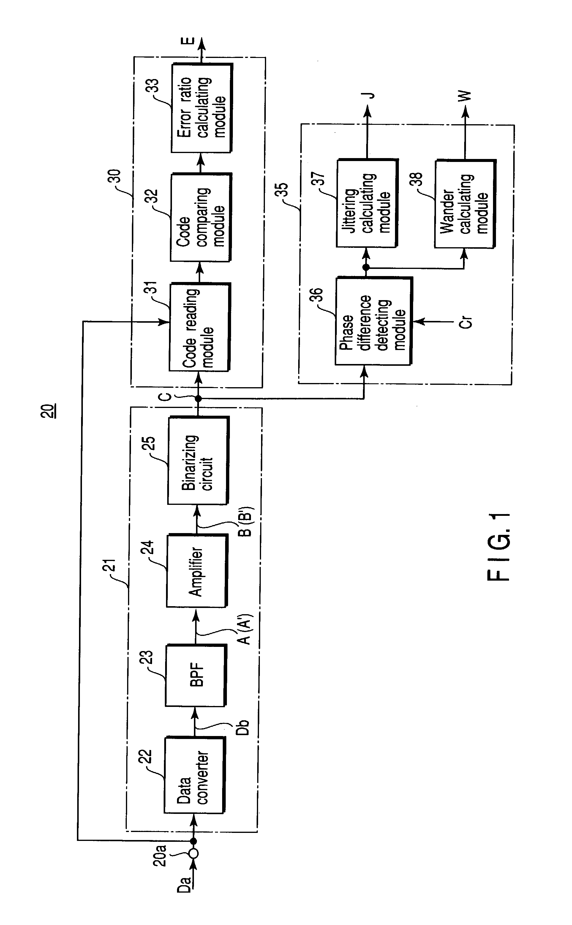
[0102] FIG. 1 is a block diagram showing a configuration of a first embodiment of a measuring device 20 and a clock regenerating circuit 21 used therein according to the present invention.
[0103] This measuring device 20 is applied to an error measurement and a jitter / wander measurement of a data transmitting system.
[0104] This measuring device 20 has the clock regenerating circuit 21, an error measuring portion 30, and a jitter / wander measuring portion 35.
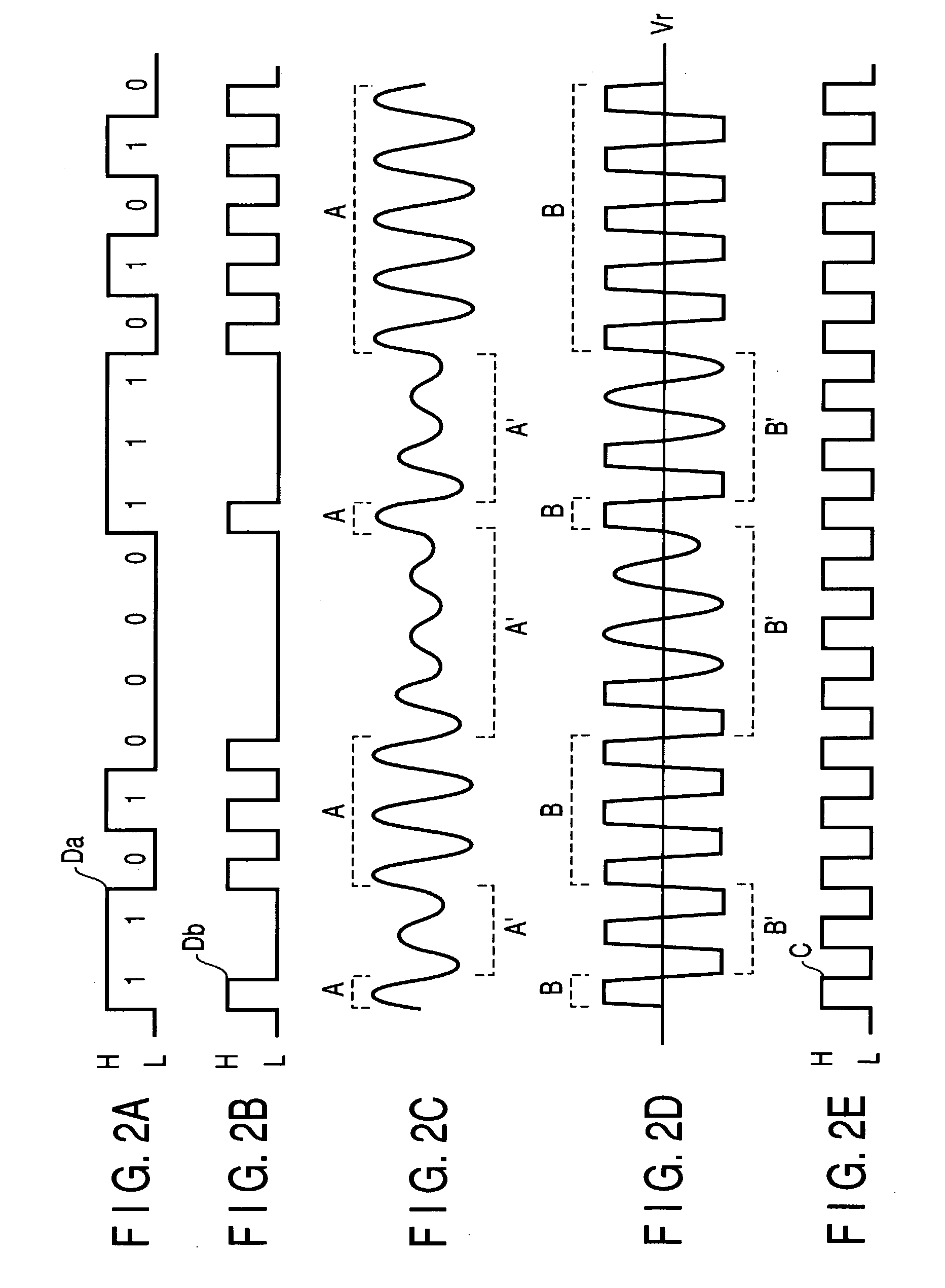
[0105] First, a data converter 22 of the clock regenerating circuit 21 converts an NRZ method data signal Da, transmitted at a predetermined carrier wave frequency inputted from an input terminal 20a, to an RZ method data signal Db.
[0106] The data signal Db outputted from the data converter 22 is inputted to a band-pass filter 23.
[0107] This band-pass filter 23 selectively extracts a signal component having a frequency which is the same as that of a clock signal to be regenerated, by a resonance element, fo...
second embodiment
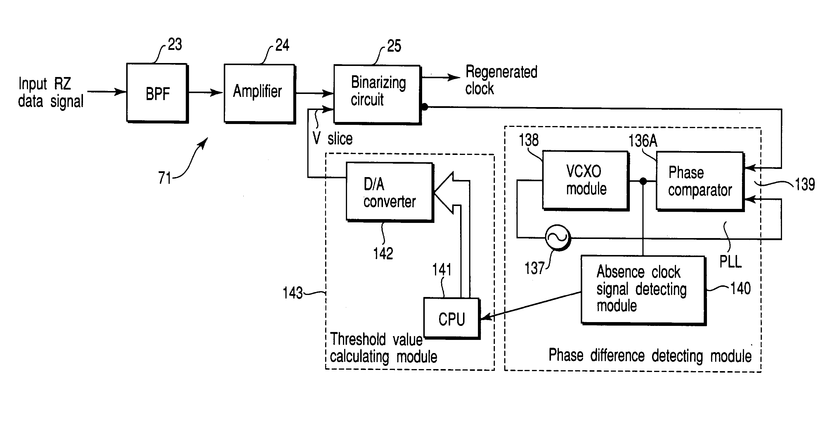
[0146] (Second Embodiment)
[0147] FIG. 4 is a block diagram showing a configuration of a second embodiment of the clock regenerating circuit for use in the measuring device according to the present invention.
[0148] In the clock regenerating circuit 21 for use in the measuring device according to the above-described first embodiment, the output signal of the binarizing circuit 25 is outputted as a clock signal component C.
[0149] However, when a sine wave shaped clock signal is needed at the error measuring portion 30 or the jitter / wander measuring portion 35, a clock regenerating circuit 41 as shown in FIG. 4 can be used.
[0150] The clock regenerating circuit 41 inputs the output signal of the binarizing circuit 25 to another band-pass filter 26 formed to be the same level as the band characteristic or the like of the band-pass filter 23, and outputs the sine wave shaped clock signal C from the band-pass filter 26.
[0151] Namely, in the clock regenerating circuit 41 used in this embodim...
third embodiment
[0152] (Third Embodiment)
[0153] FIG. 5 is a block diagram showing a configuration of a third embodiment of the clock regenerating circuit for use in the measuring device according to the present invention.
[0154] In the aforementioned clock regenerating circuits 21, 41, the RZ method data signal Db outputted from the data converter 22 is directly inputted to the band-pass filter 23.
[0155] However, when measurement of jitter having a wider band is carried out, it is necessary to widen the passage band of the band-pass filter 23 in order not to damper the jitter component. Therefore, the duration time of relaxation vibration at the interior of the band-pass filter 23 becomes much shorter correspondingly.
[0156] In such a case, for example, as in the case of a clock regenerating circuit 51 as shown in FIG. 5, a plurality of groups of the group of the band-pass filter 23, the amplifier 24, and the binarizing circuit 25 are connected in series. If the absence of the clock signal is elimina...
PUM
 Abstract
Description
Claims
Application Information