Supercharge Your Innovation With Domain-Expert AI Agents!

Antifuse Circuit

a technology of anti-fuse circuit and circuit, which is applied in the direction of static storage, electrical equipment, instruments, etc., can solve the problems of waste of memory chips with defective bits, inefficient and costly, and difficult to manufacture devices of such a high bit density, and achieve the effect of increasing the reliability of anti-fuse circui

Inactive Publication Date: 2003-11-27
SK HYNIX INC
View PDF17 Cites 10 Cited by
  • Summary
  • Abstract
  • Description
  • Claims
  • Application Information

AI Technical Summary

Benefits of technology

[0028] Therefore, an antifuse circuit is disclosed for effectively increasing the reliability of an antifuse circuit of a semiconductor device.

Problems solved by technology

However, due to the large number of bits or memory cells on each chip, it is unrealistic to assume that chips can be fabricated with every bit or memory cell position functioning.
Physical defects in the manufacturing process tend to make it very difficult to manufacture devices of such a high bit density without one or more bits or memory cells becoming defective.
Although a manufacturer cannot sell a semiconductor memory chip without ensuring that the full range of addresses is functional, discarding memory chips having defective bits is wasteful, inefficient and costly.
However, the above procedure of patching the defected semiconductor memory cell needs to be performed before packaging the memory device.
That is, using such a conventional fuse bank, it could not repair the defected semiconductor device after packaging the semiconductor memory device.
Therefore, there may be a potential problem that the unstable antifuse signal causes errors in the control of the antifuse as depicted in FIG. 3.
However, if the external voltage is applied directly to the capacitor, the reliability of the capacitor cannot be guarantied.

Method used


Image

  • Antifuse Circuit
  • Antifuse Circuit
  • Antifuse Circuit

Examples


Embodiment Construction

[0039] Other aspects of the disclosed circuits will become apparent from the following description with reference to the accompanying drawings.

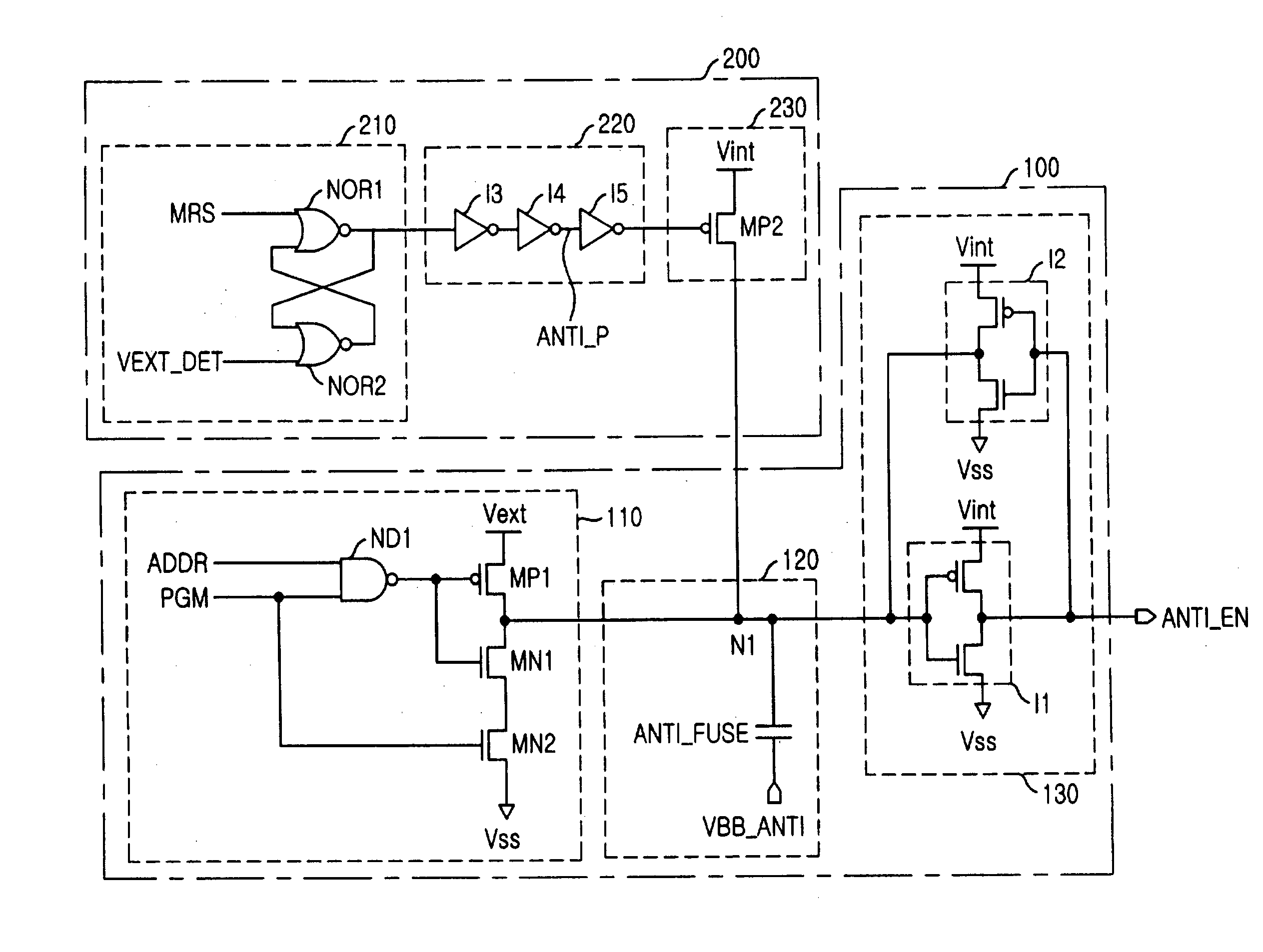
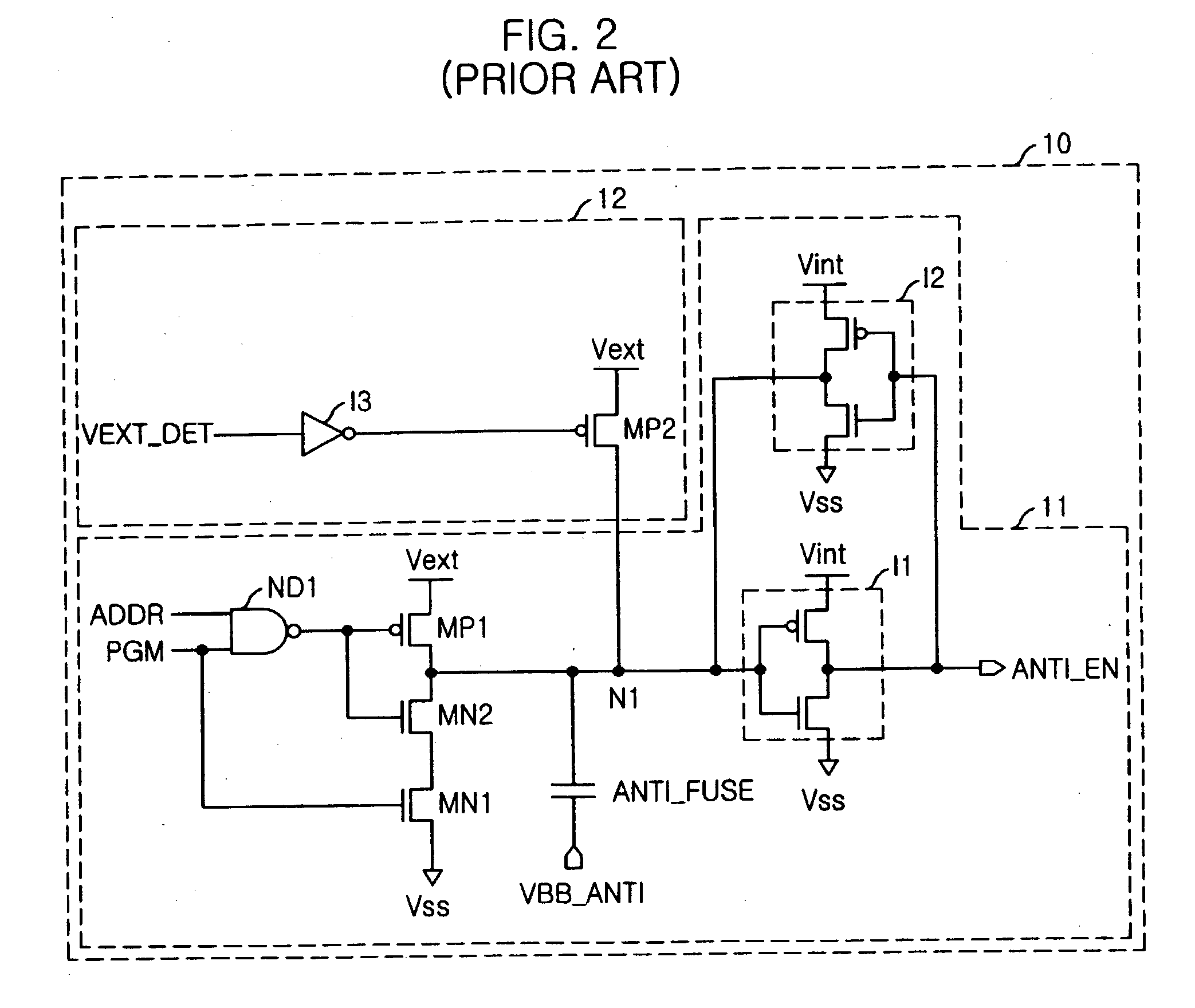
[0040] FIG. 4 is a circuit diagram showing an antifuse block in accordance with one disclosed embodiment.

[0041] As shown, the antifuse block includes an antifuse unit 100 has an antifuse ANT_FUSE, wherein the antifuse ANTI_FUSE becomes short-circuited or insulated according to a repair program, and an antifuse precharge unit 200 for latching a power-up signal VEXT_DET generated when an external voltage Vext is applied to the semiconductor device and precharging a node N1 of the antifuse as much as an internal power voltage Vint according to a latched signal.

[0042] An antifuse unit 100 includes a program unit 110, an antifuse 120 and an output latch unit 130. The program unit 110 controls the antifuse 120 by receiving two signals, a program mode selection signal PGM and an address signal ADDR. The programming unit 110 is coupled to the antifus...


PUM


Abstract

An antifuse circuit serves to generate an antifuse enable signal for use in repairing a defected memory cell in a semiconductor device. The inventive antifuse includes: an antifuse unit employing an antifuse, wherein the antifuse is controlled as being shorted or insulated according to a repair program; an antifuse precharge unit for precharging the antifuse by using a predetermined voltage level in response to a power-up signal, wherein the predetermined voltage level is lower than that of an external voltage source; and an output latch unit driven by the predetermined voltage level for latching a antifuse voltage level appearing on the antifuse and generating the antifuse enable signal corresponding to the antifuse voltage level.

Description

[0001] An antifuse circuit for use in a semiconductor memory device is disclosed which can be used as a replacement for a defective memory cell thereby making the cell operable in a more stable manner.DESCRIPTION OF RELATED ART[0002] Advances in semiconductor fabrication techniques and in a memory design have led to the commercial production of semiconductor memories, which hold millions of bits of information. It is important that a manufacturer verify that each and every bit or memory cell on a semiconductor memory chip is addressable before the chip is sold.[0003] However, due to the large number of bits or memory cells on each chip, it is unrealistic to assume that chips can be fabricated with every bit or memory cell position functioning. Physical defects in the manufacturing process tend to make it very difficult to manufacture devices of such a high bit density without one or more bits or memory cells becoming defective.[0004] Although a manufacturer cannot sell a semiconduct...

Claims


Application Information

Patent Timeline
IPC IPC(8): G11C29/00G11C17/18
CPCG11C17/18G11C29/00
Inventor LEE, KANG-YOUL
Owner SK HYNIX INC
Features
  • R&D
  • Intellectual Property
  • Life Sciences
  • Materials
  • Tech Scout
  • Unparalleled Data Quality
  • Higher Quality Content
  • 60% Fewer Hallucinations
Learn More