Magnetic storage device

a magnetic storage device and random access memory technology, applied in static storage, information storage, digital storage, etc., can solve the problem of sense operations, the magnetic field induced by the current passing only in one line is not strong enough to switch the fms, and the set-up suffers from high power consumption during write operations

Inactive Publication Date: 2004-01-29
SCHWABE NIKOLAI FRANZ GREGOE +2
View PDF4 Cites 10 Cited by
  • Summary
  • Abstract
  • Description
  • Claims
  • Application Information

AI Technical Summary

Problems solved by technology

The main disadvantage of this set-up is the relatively high power consumption during both write and sense operations due to the high conductance of the structure.
Similarly, in the other memory cells which lie along either the bit or word line used in the switching, the magnetic field induced by the current passing only in one line is not strong enough to switch the FMS.
This set-up however still suffers from high power consumption during write operations.
As a consequence of the magnetic fields of the switching currents the density of planar integration of MJT cells in an array is also limited.
Further, the supporting electric circuitry has to be designed such that both write and sense currents can be effected to flow along different paths which makes such circuitry quite complex.

Method used


Image

  • Magnetic storage device
  • Magnetic storage device
  • Magnetic storage device

Examples


Embodiment Construction

[0025] Further embodiments of the present invention shall now be described with reference to the accompanying drawings in which:

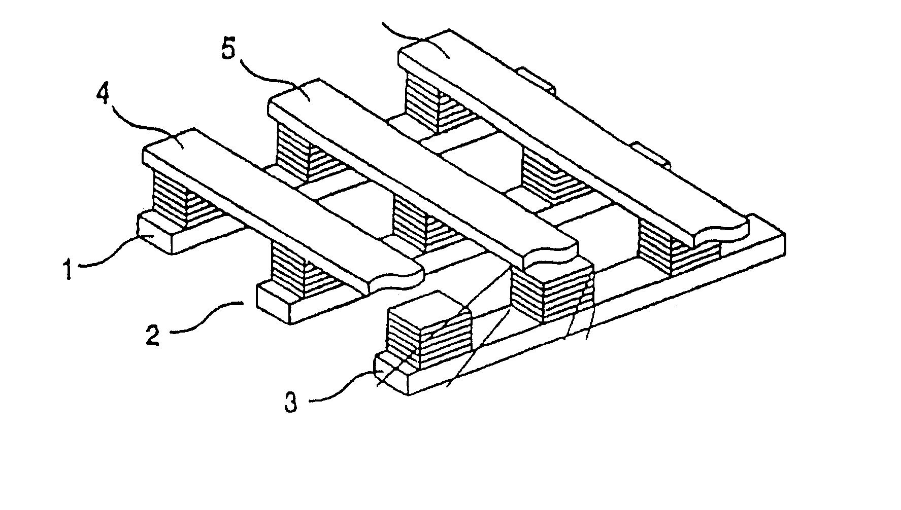
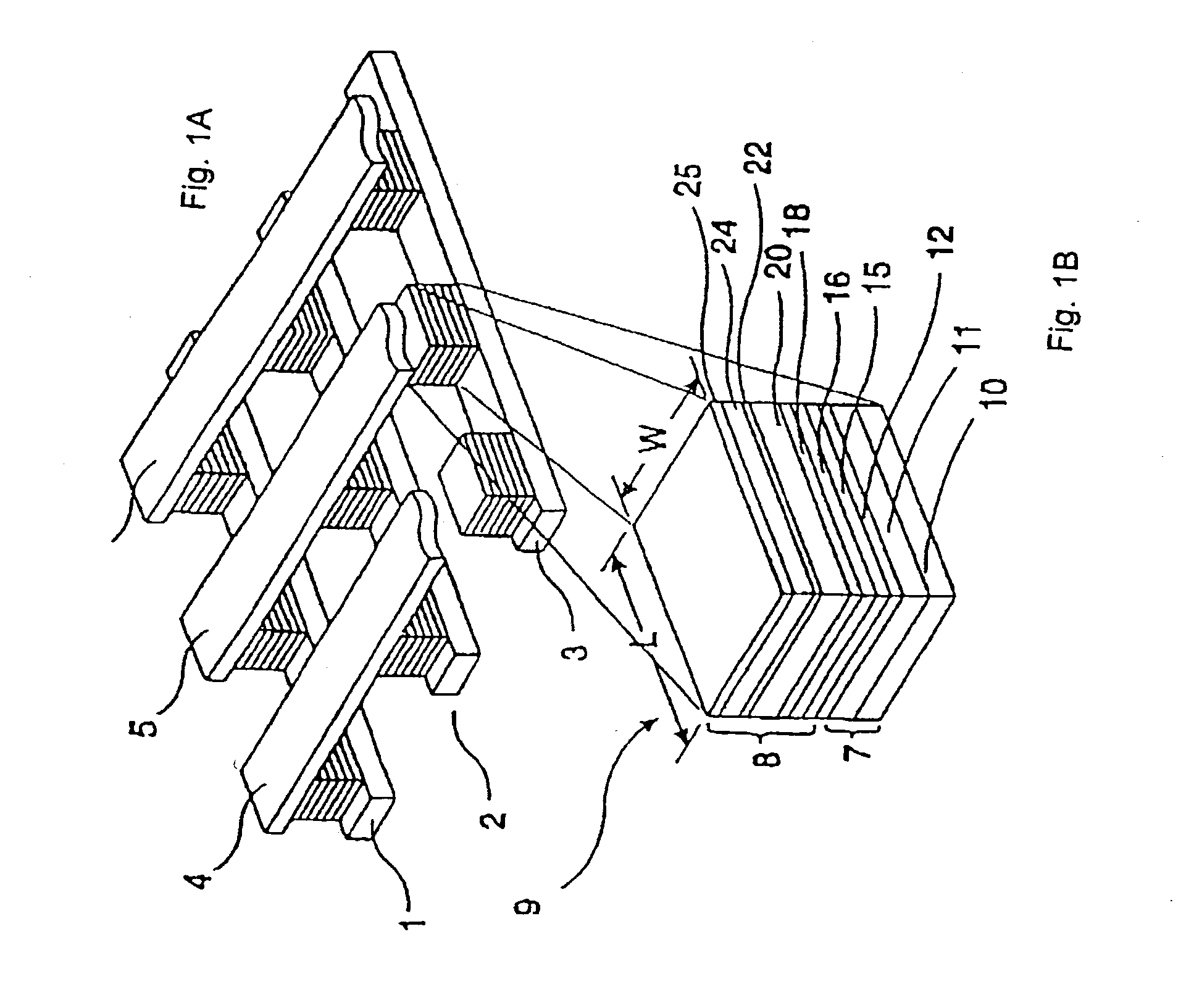
[0026] FIG. 1A shows a perspective view of a MRAM array with magnetic memory cells located vertically between bit and word lines,

[0027] FIG. 1B shows an enlarged view of one of the memory cells shown in FIG. 1A,

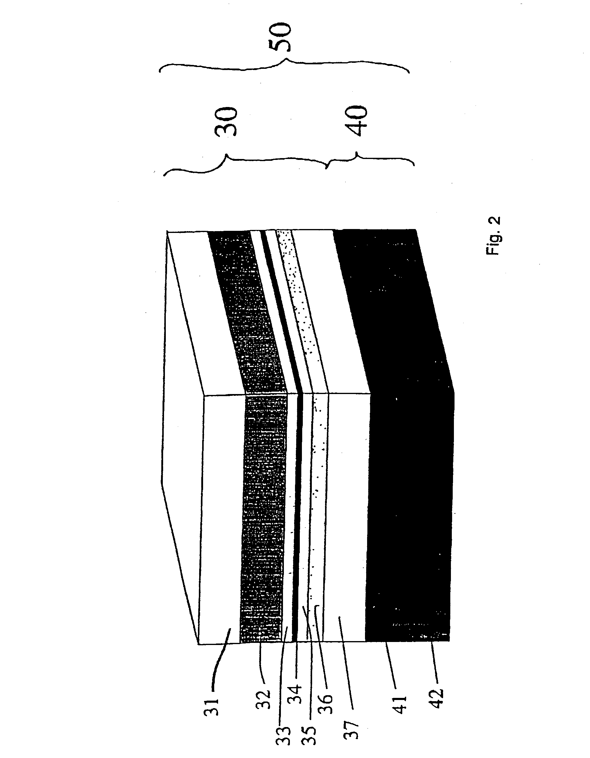
[0028] FIG. 2 shows a perspective view of a memory cell according to the present invention,

[0029] FIG. 3 shows the exchange field--voltage response of an MTJ memory cell in relation to the coercive field H.sub.C of the FMS according to the invention,

[0030] FIG. 4 shows schematically the diagram of the electric circuit formed by the MRAM array, and

[0031] FIG. 5 illustrates the voltage levels on the leads in the MRAM array according to the invention.

[0032] FIG. 1A and FIG. 1B have already been described.

CONSTRUCTION AND OPERATION OF THE MEMORY CELL

[0033] The memory cell 50 in FIG. 2 is formed as a series of layers similar to the one disclosed in U.S. P...


PUM


Abstract

A magnetic storage device comprises an array of magnetic memory cells (50). Each cell (50) has, in electrical series connection, a magnetic tunnel junction (MTJ) (30) and a Zener diode (40). The MTJ (30) comprises, in sequence, a fixed ferromagnetic layer (FMF) (32), a non-magnetic spacer layer (33), a tunnel barrier layer (34), a further spacer layer (35), and a soft ferromagnetic layer (FMS) (36) that can change the orientation of its magnetic moment. The material type and thickness of each layer in the MTJ (30) is selected so that the cell (50) can be written by applying a voltage across the cell, which sets the orientation of the magnetic moments of the FMF (32) and FMS (36) relative to one another. The switching is effected by means of an induced exchange interaction between the FMS and FMF mediated by the tunneling of spin-polarised electrons in the MTJ (30). The cell (50) therefore has low power consumption during write operations allowing for fast writing and dense integration of cells (50) in an array. The mechanism used to control the array to write and sense the information stored in the cells (50) is simplified.

Description

DESCRIPTION[0001] 1. Field of the Invention[0002] The present invention relates to non-volatile magnetic random access memory (MRAM) storage elements.[0003] 2. Background of the Invention[0004] Important characteristics of mass information storage devices of the future should be high speed, low power consumption, low cost and small size. To achieve this aim, magnetic random access memories (MRAMs) have been proposed due to their non-volatile nature. Unlike dynamic random access memory (DRAM) cells, non-volatile memory cells such as MRAM cells do not require a complex circuitry for perpetual electronic refreshing of the information stored, and thus can in principle outperform DRAM cells in all above mentioned characteristics.[0005] The first of such MRAMs were based on magnetic multi-layer structures, deposited on a substrate. U.S. Pat. No. 5,343,422, for example, discloses a structure in which two layers of ferromagnetic material are separated by a layer of non-magnetic metallic con...

Claims


Application Information

Patent Timeline
Patent Type & Authority Applications(United States)
IPC IPC(8): G11C11/16
CPCG11C11/16
Inventor SCHWABE, NIKOLAI FRANZ GREGOEHEIDE, CARSTENELLIOTT, ROGER JAMES
Owner SCHWABE NIKOLAI FRANZ GREGOE
Why Eureka
Try Eureka