Tri-gate devices and methods of fabrication

a technology of tri-gate and substrate, applied in the direction of semiconductor devices, electrical equipment, nanotechnology, etc., can solve the problems of increasing impracticality, decreasing the thickness of silicon films, and reducing the production efficiency of thin silicon films with thicknesses less than 10 nanometers, and is considered to be extremely difficul

Inactive Publication Date: 2004-02-26
INTEL CORP
View PDF98 Cites 553 Cited by
  • Summary
  • Abstract
  • Description
  • Claims
  • Application Information

AI Technical Summary

Problems solved by technology

However, as gate lengths scale especially as they approach 30nm, the need for ever decreasing silicon film thickness (Tsi) makes this approach increasingly impractical.
The fabrication of thin silicon films with thicknesses of less than 10 nanometers, is considered to be extremely difficult.
On one hand, obtaining wafer uniformity on the order of one nanometer is a difficult challenge.
On the other hand, to be able to contact these thin films to form raised source / drain regions to decrease junction resistance, becomes almost impossible since the thin silicon layer in the source / drain regions becomes consumed during the gate etch and various cleans following the gate etch and spacer etch leaving insufficient silicon 106 for silicon to grow on.
Although, double gate structures double the thickness of the silicon film (since there now is a gate on either side of the channel) these structures, however, are hideously difficult to fabricate.

Method used


Image

  • Tri-gate devices and methods of fabrication
  • Tri-gate devices and methods of fabrication
  • Tri-gate devices and methods of fabrication

Examples


Embodiment Construction

[0015] The present invention is a novel tri-gate transistor structure and its method of fabrication. In the following description numerous specific details are set forth in order to provide a thorough understanding in the present invention. In other instances, well-known semiconductor process and manufacturing techniques have not been described in particular detail in order to not unnecessarily obscure the present invention.

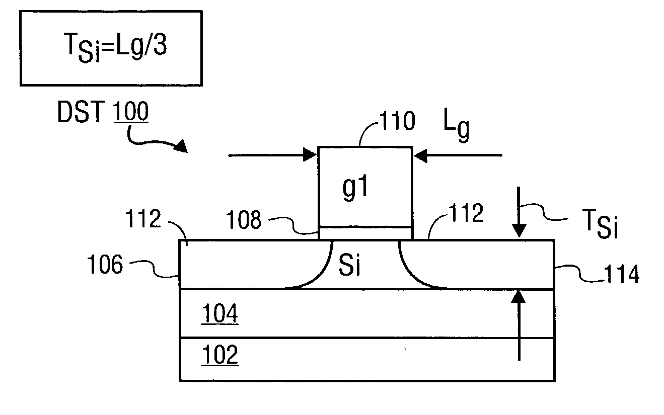
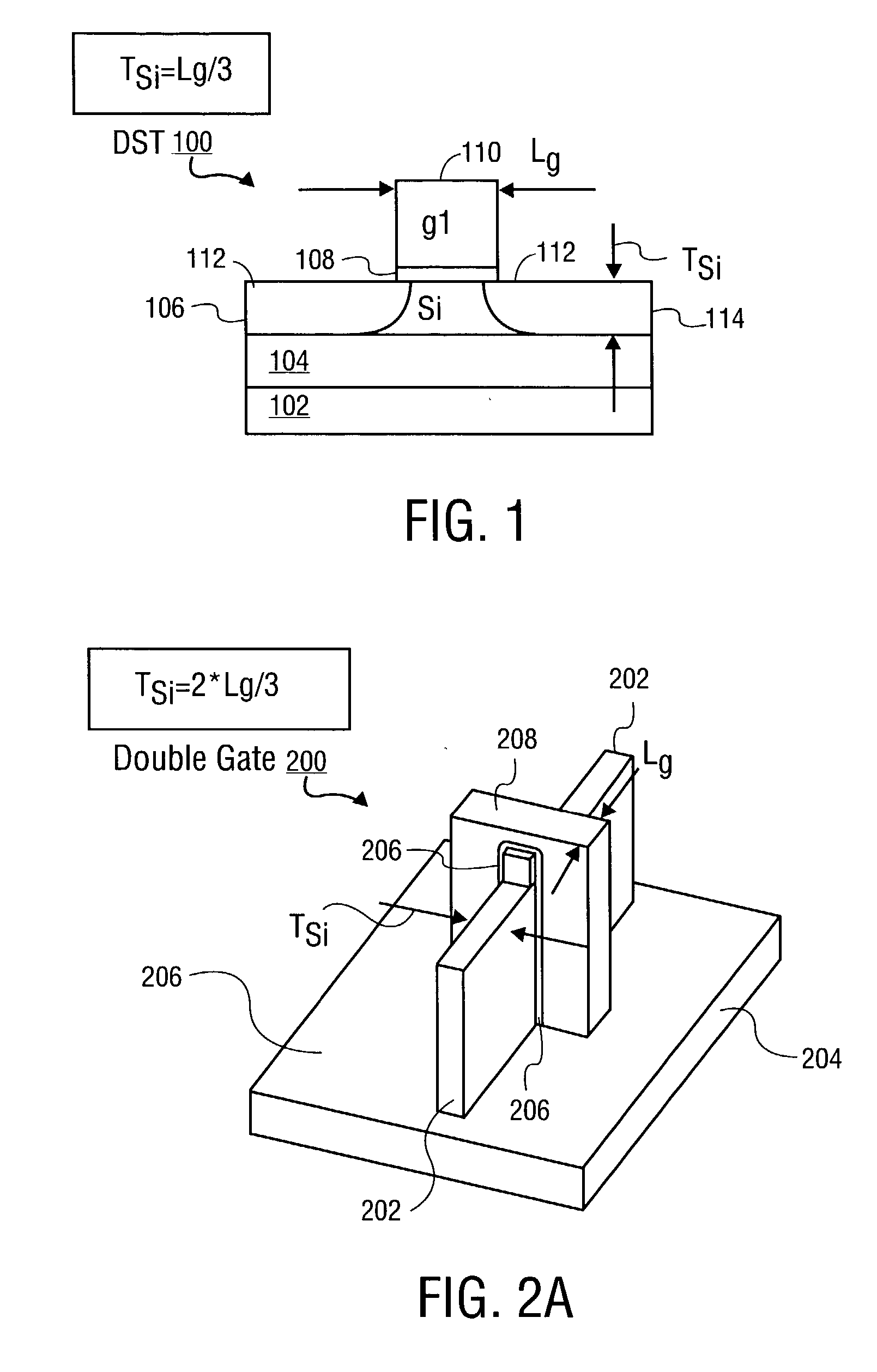
[0016] The present invention is novel tri-gate transistor structure and its method of fabrication. In an embodiment of the present invention, the tri-gate transistor is a semiconductor on insulator (SOI) transistor. The tri-gate transistor is ideal for use in fully depleted substrate transistor applications. The tri-gate transistor includes a thin semiconductor body formed on an substrate, the substate can be an insulating substrate or a semiconductor substrate. A gate dielectric is formed on the top surface and the sidewalls of the semiconductor body. A gate ele...


PUM


Abstract

The present invention is a semiconductor device comprising a semiconductor body having a top surface and laterally opposite sidewalls formed on a substrate. A gate dielectric layer is formed on the top surface of the semiconductor body and on the laterally opposite sidewalls of the semiconductor body. A gate electrode is formed on the gate dielectric on the top surface of the semiconductor body and adjacent to the gate dielectric on the laterally opposite sidewalls of the semiconductor body.

Description

[0001] 1. Field of the Invention[0002] The present invention relates to the field of semiconductor integrated circuit manufacturing, and more particularly to a tri-gate fully depleted substrate transistor and its methods of fabrication.[0003] 2. Discussion of Related Art[0004] In order to increase device performance, silicon on insulator (SOI) transistors have been proposed for the fabrication of modern integrated circuits. FIG. 1 illustrates a standard fully depleted silicon on insulator (SOI) transistor 100. SOI transistor 100 includes a single crystalline silicon substrate 102 having an insulating layer 104, such as a buried oxide formed thereon. A single crystalline silicon body 106 is formed on the insulating layer 104. A gate dielectric layer 108 is formed on the single crystalline silicon body 106 and a gate electrode 110 formed on the gate dielectric 108. Source 112 and drain 114 regions are formed in the silicon body 106 along laterally opposite sides of gate electrode 1 10...

Claims


Application Information

Patent Timeline
Patent Type & Authority Applications(United States)
IPC IPC(8): H01L21/336H01L29/423H01L29/786
CPCB82Y10/00H01L29/78696H01L29/0673H01L29/1033H01L29/42384H01L29/42392H01L29/4908H01L29/66795H01L29/772H01L29/785H01L29/7854H01L29/78645H01L51/0048H01L51/0554Y10S977/742Y10S977/842Y10S977/938H01L29/41791H01L29/0665H10K85/221H10K10/482
Inventor CHAU, ROBERT S.DOYLE, BRIAN S.KAVALIEROS, JACKBARLAGE, DOUGLASDATTA, SUMAN
Owner INTEL CORP
Why Eureka
Try Eureka