Wafer burn-in and test employing detachable cartridge
a detachable cartridge and wafer technology, applied in the field of wafers, can solve the problems of ic's, prone to fail early in their projected life, and loss of added packaging costs,
- Summary
- Abstract
- Description
- Claims
- Application Information
AI Technical Summary
Benefits of technology
Problems solved by technology
Method used
Image
Examples
Embodiment Construction
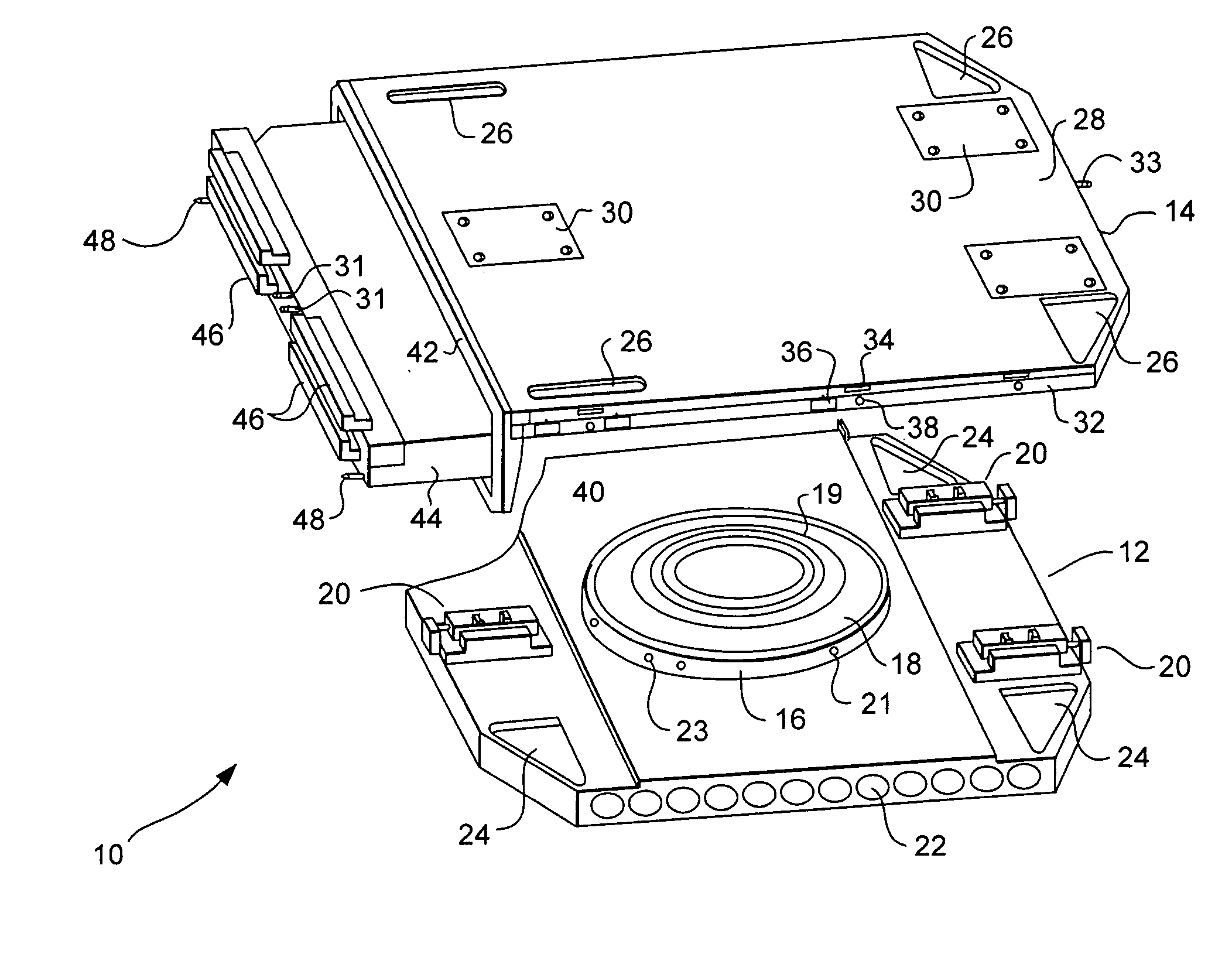
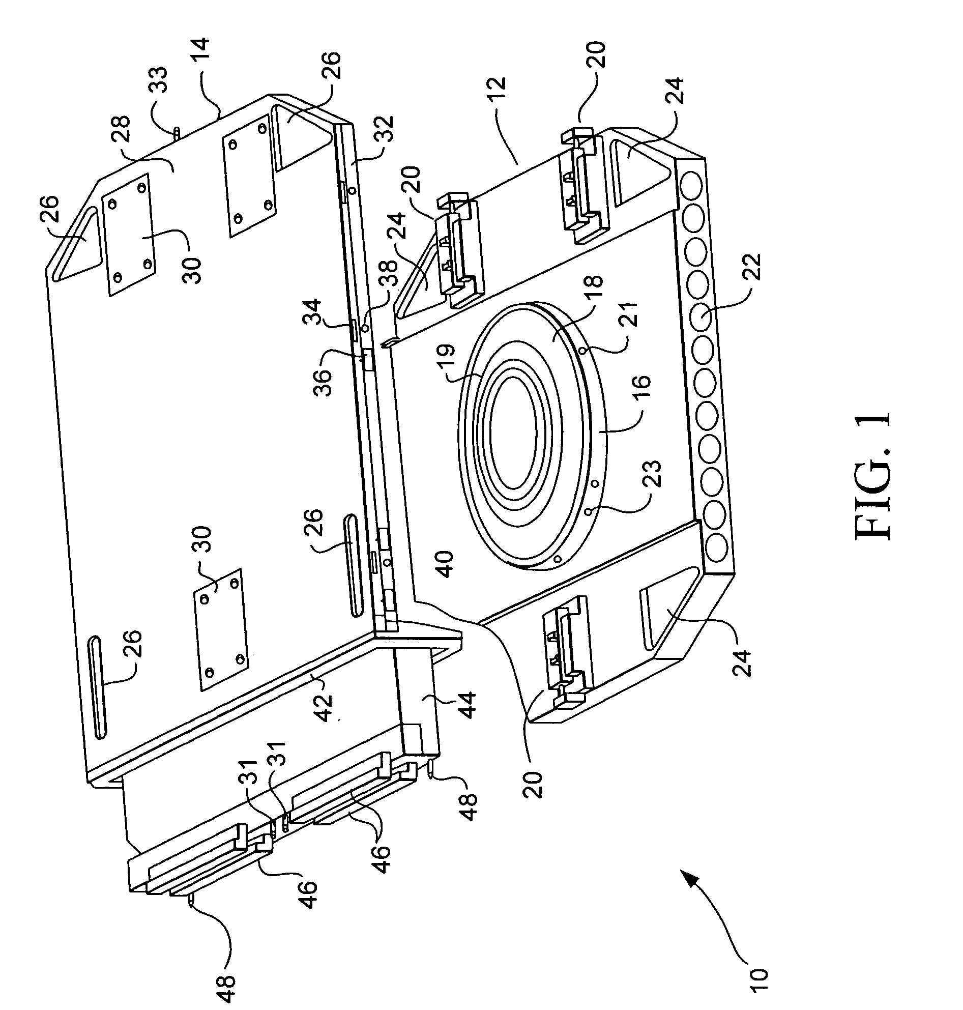
[0038] A wafer-level burn-in and test cartridge according to the invention is illustrated in FIG. 1. The cartridge, generally indicated by the reference numeral 10, comprises a chuck plate 12 and a probe plate 14. The chuck plate 12 and the probe plate 14 may be made of any suitable material. In the illustrated embodiment, the chuck plate 12 and the probe plate 14 are made of 6061 aluminum.
[0039] The chuck plate 12 is generally rectangular in shape, and includes a centrally-located raised pedestal 16. In use, a semiconductor wafer is placed on the upper surface 18 of the pedestal 16. Mounted to the upper surface of the chuck plate 12 are the lower halves 20 of three mechanical connecting devices that are used to lock the chuck plate 12 and the probe plate 14 together in use. In the illustrated embodiment, the mechanical connecting devices are kinematic couplings, which are discussed below in more detail with reference to FIGS. 6 to 12. Formed transversely through the chuck plate 12 ...
PUM
 Abstract
Description
Claims
Application Information


