Data inversion circuit and semiconductor device

a data inversion circuit and semiconductor technology, applied in semiconductor devices, digital data processing details, instruments, etc., can solve problems such as posing marked difficulties in timing design

Active Publication Date: 2004-04-08
LONGITUDE LICENSING LTD
View PDF1 Cites 27 Cited by
  • Summary
  • Abstract
  • Description
  • Claims
  • Application Information

AI Technical Summary

Benefits of technology

0070] FIG. 8 is a block diagram showing a con...

Problems solved by technology

It should be noted that, when the conventional data inversion circuit is applied to a semiconductor device operating at a high speed clock rate, such as, for example, a double data rate synchronous dynamic random access memory (DDR-SDRAM), the following problem is encounter...

Method used


Image

  • Data inversion circuit and semiconductor device
  • Data inversion circuit and semiconductor device
  • Data inversion circuit and semiconductor device

Examples


embodiment 1

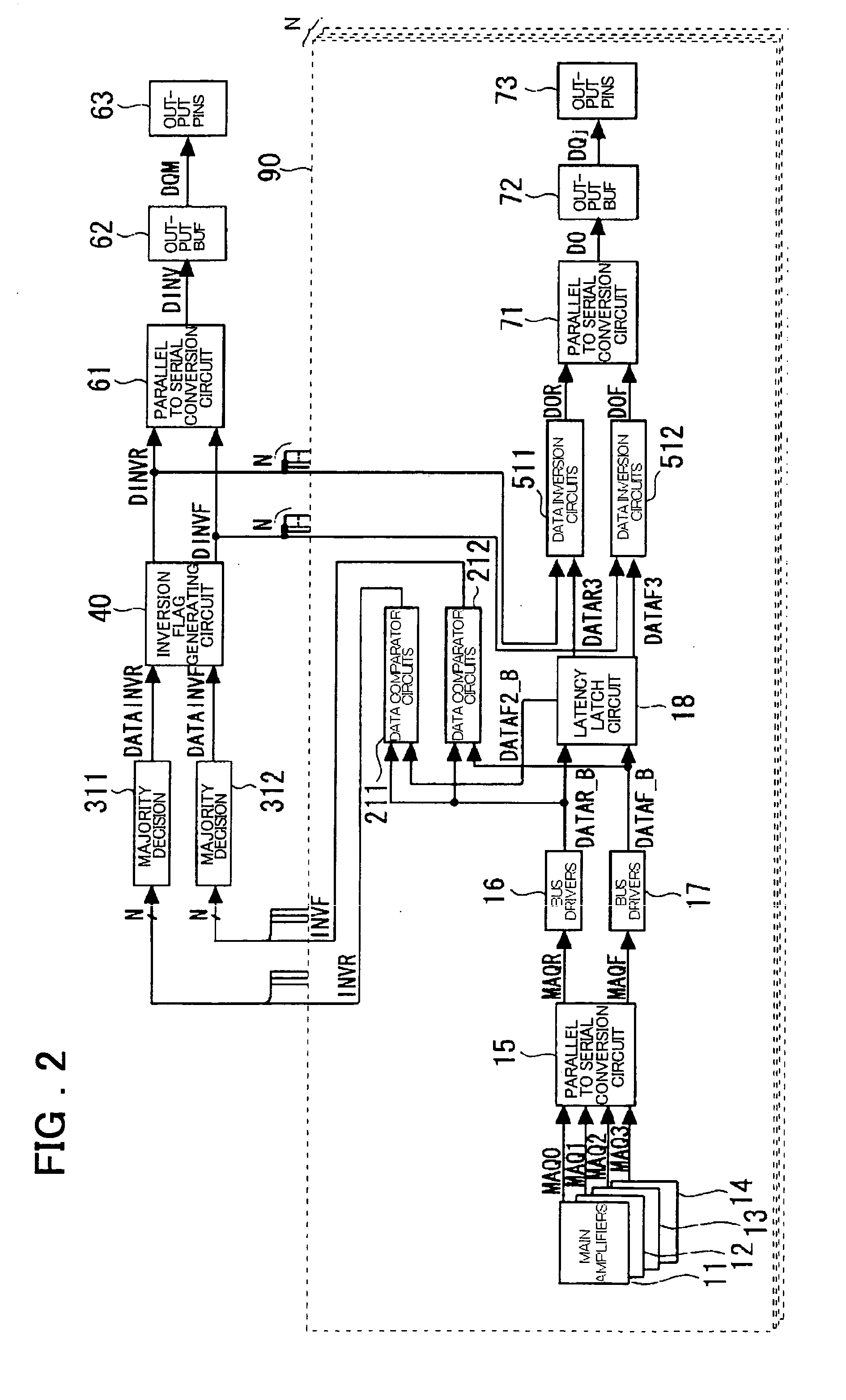
[0085] [Embodiment 1]

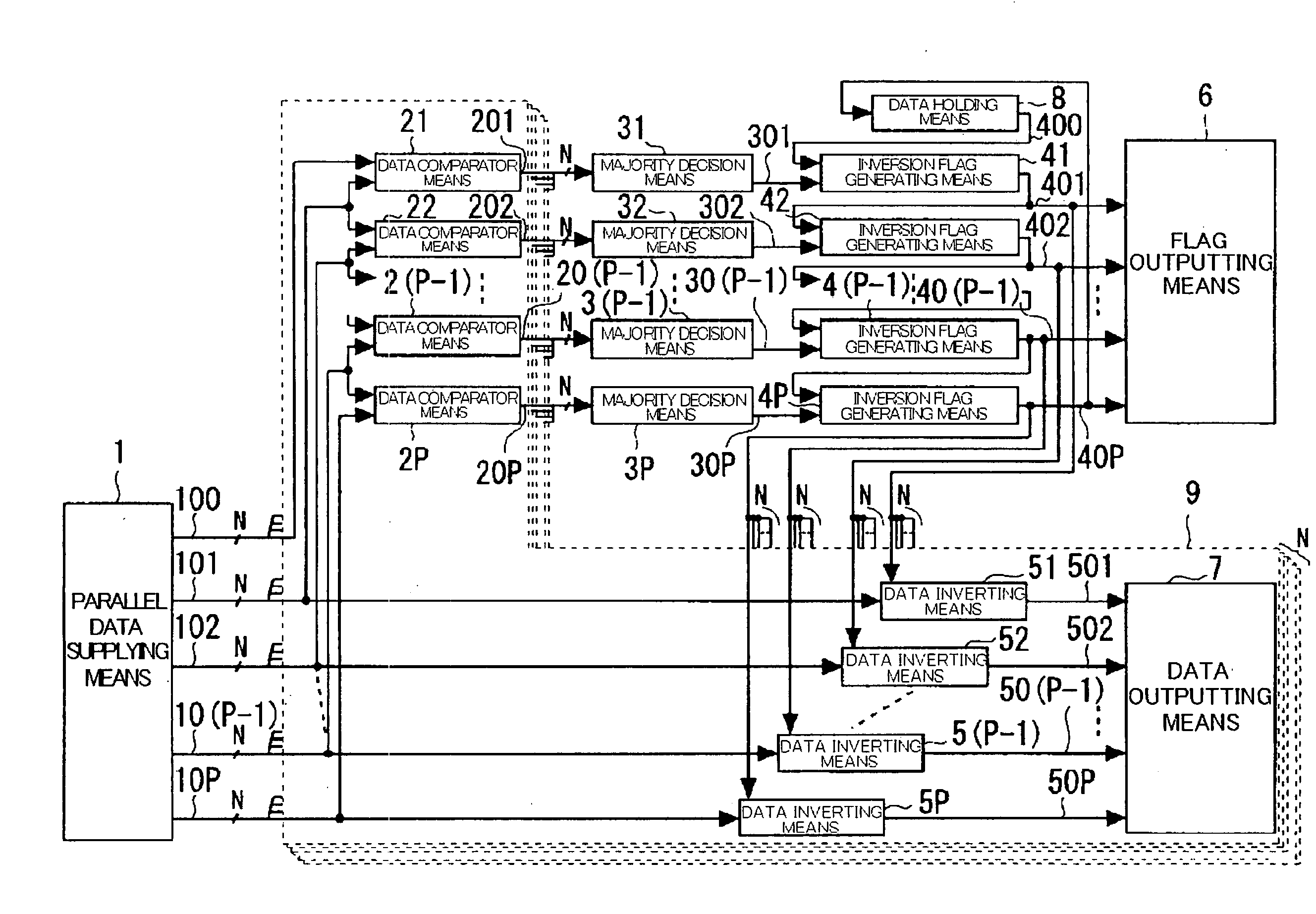
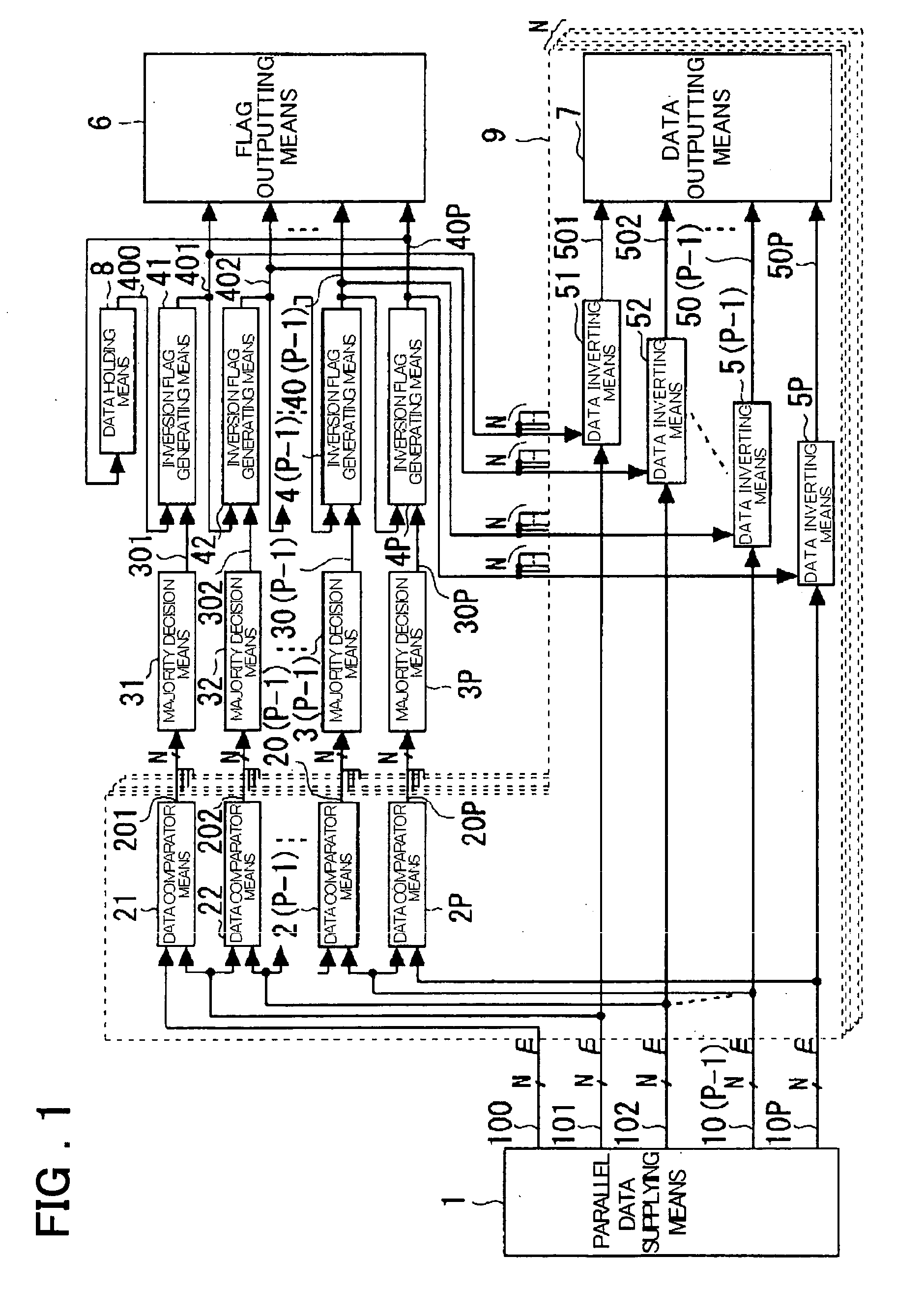
[0086] FIG. 2 is a block diagram showing the configuration of a data inversion circuit according to a first embodiment of the present invention, where P=2. Referring to FIG. 2, the data inversion circuit according to the first embodiment of the present invention comprises main amplifiers 11 to 14, a parallel-to-serial conversion circuits 15, bus drivers 16 and 17, a latency latch circuit 18, data comparator circuits 211 and 212, majority decision circuits 311 and 312, an inversion flag generating circuit 40, data inversion circuits 511 and 512, parallel to serial conversion circuits 61 and 71, output buffer circuits 62 and 72, and output pins 63 and 73.

[0087] Meanwhile, a data read unit 90, which is composed by the main amplifiers 11 to 14, parallel-to-serial conversion circuit 15, bus drivers 16 and 17, latency latch circuit 18, data comparator circuits 211 and 212, data inversion circuits 511 and 512 parallel to serial conversion circuit 71, output buffer circ...

embodiment 2

[0135] [Embodiment 2]

[0136] FIG. 7 is a block diagram showing the configuration of a data inversion circuit according to a second embodiment of the present invention, with P=4. FIG. 7 shows the connection of plural blocks of a data comparator circuit, a majority decision circuit and an inversion flag generating circuit, as major portions of the data inversion circuit, and thus depicts an illustrative circuit structure having four serial channels or paths.

[0137] There are provided exclusive-OR (Ex-OR) circuits 213, 214, 215 and 216, corresponding to data comparator circuits, and which are present in association with a preset one bit of N-bit parallel data, where N is an integer not less than 2. There are also provided exclusive-OR (Ex-OR) circuits 413, 414, 415 and 416, corresponding to the inversion flag generating circuit. A D-latch circuit 418 holds the inversion flag signal DINV3, output by the Ex-OR circuit 416, by a timing circuit, not shown, or by clock signals K, supplied by ...


PUM


Abstract

A parallel data outputting circuit equipped with a data inversion function, comprises P number of data comparator means, P number of majority decision circuits, P number of inversion flag generating means and P number of data inversion circuits, these being activated in parallel in one cycle. In generating an inversion flag indicating whether or not the parallel data are to be inverted and output in the inverted state, inversion flags are calculated from outputs of the inversion flag generating means and the inversion flag generating means of a cycle directly previous to a current cycle.

Description

[0001] This invention relates to a data inversion circuit for temporally sequentially outputting multi-bit parallel data. More particularly, it relates to a data inversion circuit suitable for a read circuit of a clock synchronized semiconductor memory device, and to a semiconductor device employing the data inversion circuit.[0002] In an electronic device which outputs multi-bit data in parallel, the noise generated at the time of data transition poses a problem. This noise is produced most severely at the time of a transition corresponding to the switching of a CMOS logic circuit and the large amount of power is dissipated at the time of the transition. As a technique for reducing the number of transition times of the output data signals at the time of switching in a logic circuit, there is known a function of data inversion. This data inversion is of such a function in which data of a given cycle is compared to data output in a directly previous cycle and, in case the major part ...

Claims


Application Information

Patent Timeline
IPC IPC(8): G11C11/409G06F3/00G06F7/06G06F13/42G11C7/00G11C11/00G11C11/407H01L31/109
CPCG11C7/1006G11C7/02
Inventor YOSHIDA, HIROYASUOISHI, KANJI
Owner LONGITUDE LICENSING LTD
Why Eureka
Try Eureka