Semiconductor storage device

a technology of semiconductors and storage devices, applied in the direction of digital storage, electronic circuit testing, instruments, etc., can solve the problems of complex testing operations, and achieve the effect of improving testability

Inactive Publication Date: 2004-10-14
LONGITUDE LICENSING LTD
View PDF12 Cites 32 Cited by
  • Summary
  • Abstract
  • Description
  • Claims
  • Application Information

AI Technical Summary

Benefits of technology

0021] It is therefore a principal object of the present invention to provide a semiconductor storage device in which it is possible to prevent the c

Problems solved by technology

The result is complex testing operations for tests

Method used


Image

  • Semiconductor storage device
  • Semiconductor storage device
  • Semiconductor storage device

Examples


Embodiment Construction

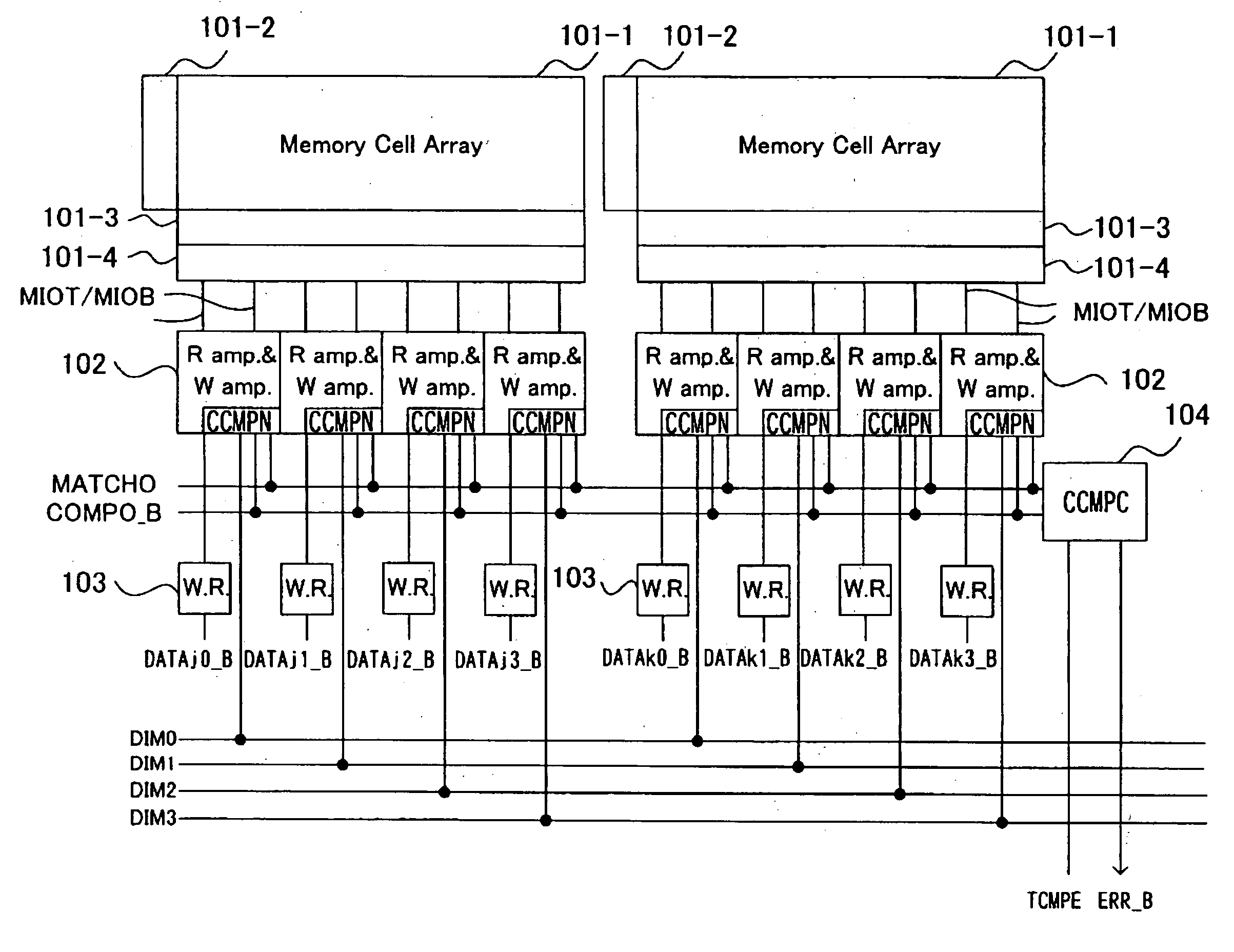
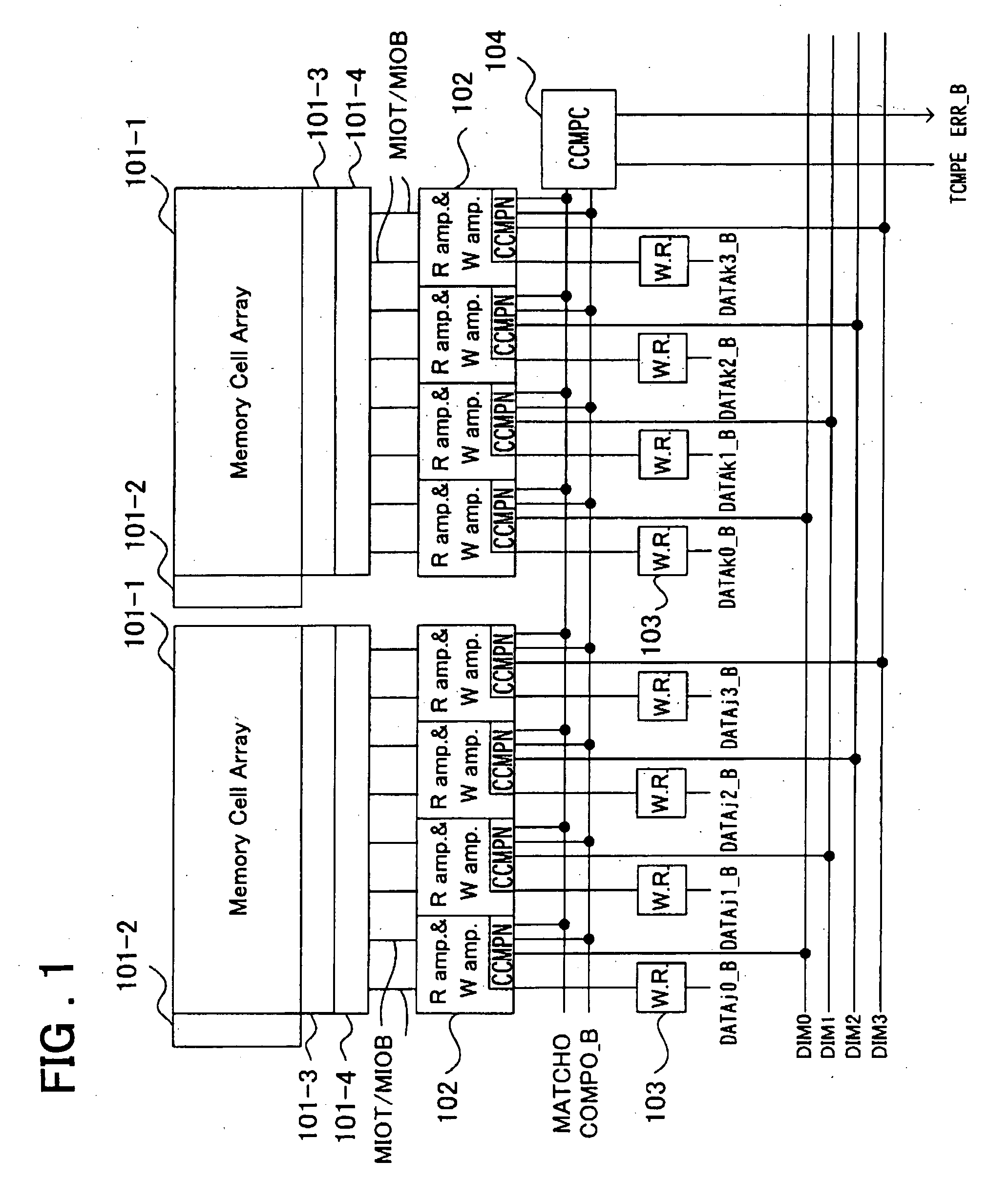
[0042] An embodiment of the present invention is now explained. Referring to FIG. 1, a semiconductor storage device in one aspect of the present invention includes a memory cell array (101-1) including a plurality of memory cells, a holding circuit (103) for holding data written in the memory cells, a comparator (CCMPN) for comparing readout data from the memory cell and expectation data corresponding to the readout data, supplied thereto, in order to check whether or not the two coincide with each other, and an inversion control circuit (see FIG. 3) for outputting an inverted value or a non-inverted value of data held by the holding circuit (103), responsive to the value of an inversion control signal (DIM) supplied thereto along with the data held by the holding circuit (103). An output from the inversion control circuit is supplied as write data to the memory cell and supplied as the expectation data to the comparator (CCMPN).

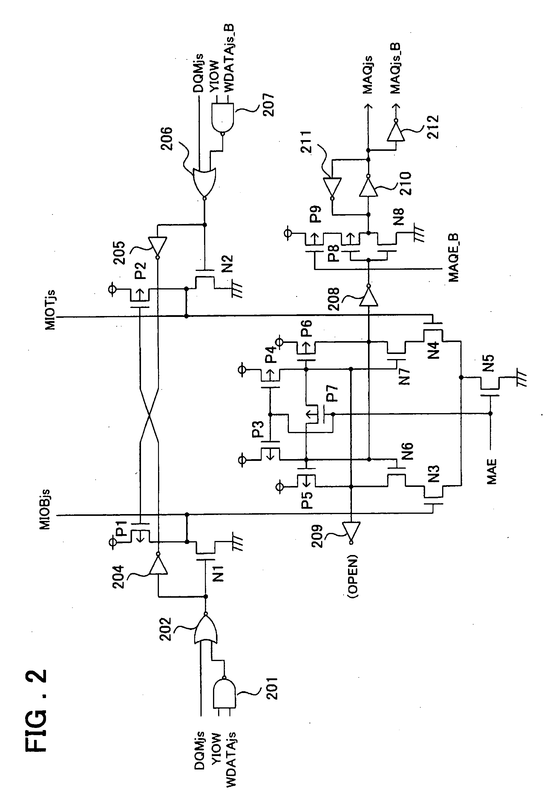
[0043] In an embodiment of the present invention, the ...


PUM


Abstract

A testing device for a semiconductor storage device which suppresses the increase in the circuit size, provides for facilitated accommodation to a test with frequent changes in the test pattern, and which improves testability of the semiconductor storage device. A plural number of holding circuits (103) are provided holding write data for memory cells of a memory cell array (101-1). The write data from the holding circuits (103) are written in the memory cells of the selected address. A plural number of comparators (CCMPN) are supplied with data read out from the memory cells and with data held by the holding circuits as expectation data to compare the readout data and the expectation data. The non-inverted value or the inverted value of the write data held by the holding circuits (103) is output as the write data to the memory cells and as expectation data to the comparators (CCMPN) depending on the value of the inversion control signal (DIM). A decision circuit (104) is provided which outputs an error flag based on a coincidence detection signal (MATCH0) coupled to the plural comparators.

Description

[0001] This invention relates to a semiconductor storage device and, more particularly, to a semiconductor storage device convenient for parallel testing employing a testing device.[0002] As a parallel test, employing a testing device, a line mode test for semiconductor devices has become known (see for example the non-patent publication 1). First, the line mode test is briefly explained. FIG. 13 shows the structure of a semiconductor storage device disclosed in the non-patent publication 1. The storage device shown in FIG. 13 includes a multi-purpose register MPR (write / expectation value register) 1101 and a comparator circuit 1102 for complementary sub-IO lines SIO_T, SIO_B (bit line pair). The comparator circuit 1102 is formed by an Ex-OR circuit, and an output signal (coincidence detection signal) MATCH is wired-OR connected. The multi-purpose register MPR 1101, comprising a flip-flop formed by cross-connection of an output and an input of an inverter composed of a P-channel MOS...

Claims


Application Information

Patent Timeline
IPC IPC(8): G11C11/401G01R31/28G11C29/26G11C29/34
CPCG11C2029/2602G11C29/26
Inventor YOSHIDA, HIROYASUOISHI, KANJI
Owner LONGITUDE LICENSING LTD
Why Eureka
Try Eureka