Method and Circuit Arrangement for Performing a Write Through Operation, and SRAM Array With Write Through Capability

a write through operation and circuit arrangement technology, applied in the field of digital memory circuits, can solve the problems of high cost and inability to read the global bit line correctly, so as to improve the observability and testability of the circuit, prevent false write through data propagation, and improve the effect of finding and screening out failing parts

Inactive Publication Date: 2011-12-29
IBM CORP
View PDF0 Cites 12 Cited by
  • Summary
  • Abstract
  • Description
  • Claims
  • Application Information

AI Technical Summary

Benefits of technology

All in all, embodiments of the present invention address the false write through propagation problem of a SRAM cell with write-through capability. The core idea of the present invention is to implement a method and / or a circuit arrangement for performing a write through operation during a write operation of a SRAM cell in high performance / low power SRAM arrays using a dual local bit line / dual local word line approach and providing one write or two read port operation per cycle. The primary focus of this invention is to provide a method and / or a circuitry for preventing false write through data from propagating to the array outputs during a write operation. In opposite to state of the art write bypass or write around schemes this invention uses the read data propagation paths to provide write through functionality in order to improve observability and testability of the circuit. By using the read data propagation paths it is advantageously possible to test the full latch to latch paths that are used in the chip function at the same frequency that will be used in the system application. So the efficiency in finding and screening out failing parts is advantageously increased.

Problems solved by technology

If the circuits are tested at a slower frequency or part of the functional path is bypassed, then there could be delay defects that would not be caught by test but result in a failing chip when exercised in the system.
This is a very expensive point to find and screen out failing parts.
This discharge of the global bit line will be impossible to recover from until the next cycle, thereby resulting in an incorrect value being read on the global bit line during the “write-through” operation.
This “False Write Through Propagation problem” cannot be suppressed with current implementations.
In state of the art solutions cross coupled PFETs are suppressing false write through propagation in single read port designs, but this is not possible for supporting two independent read ports since independent bit lines are needed to employ independent read ports.

Method used


Image

  • Method and Circuit Arrangement for Performing a Write Through Operation, and SRAM Array With Write Through Capability
  • Method and Circuit Arrangement for Performing a Write Through Operation, and SRAM Array With Write Through Capability
  • Method and Circuit Arrangement for Performing a Write Through Operation, and SRAM Array With Write Through Capability

Examples


Embodiment Construction

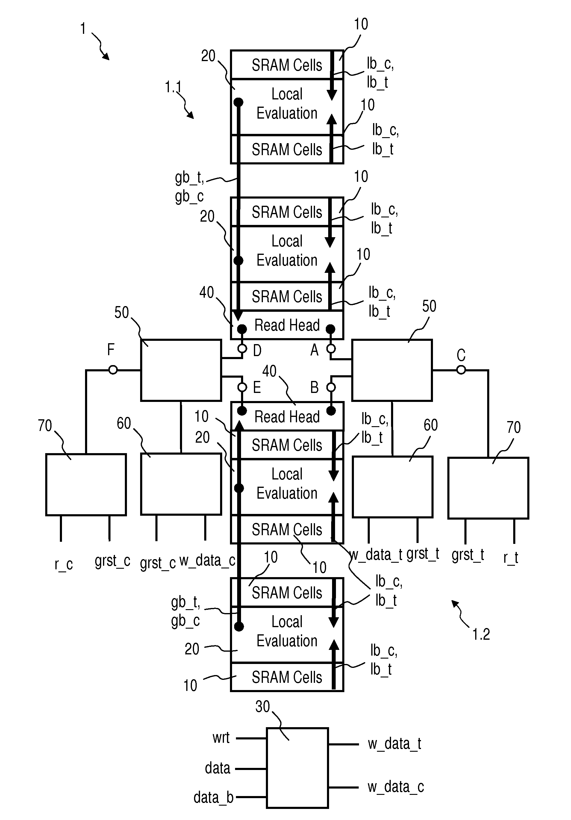
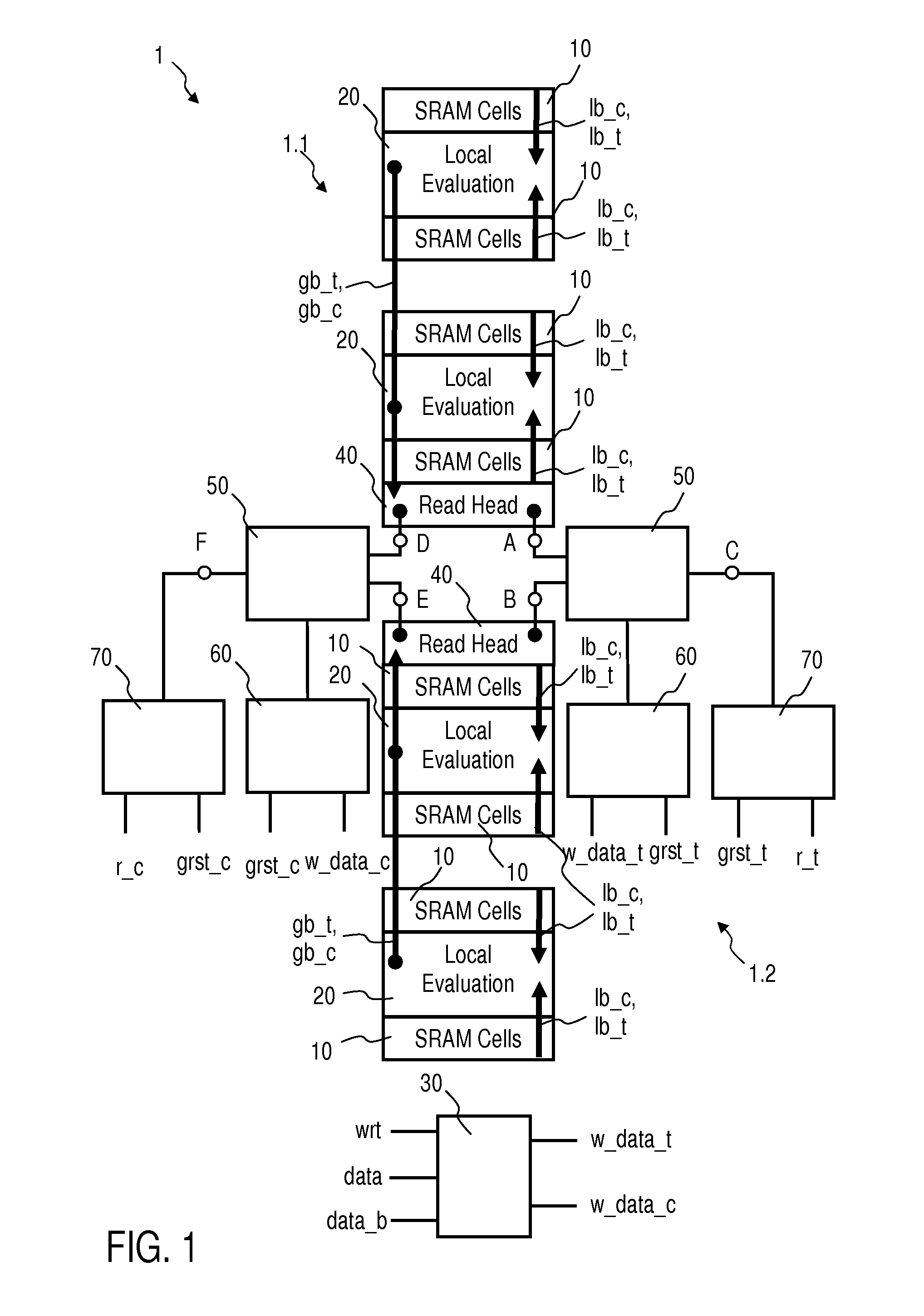
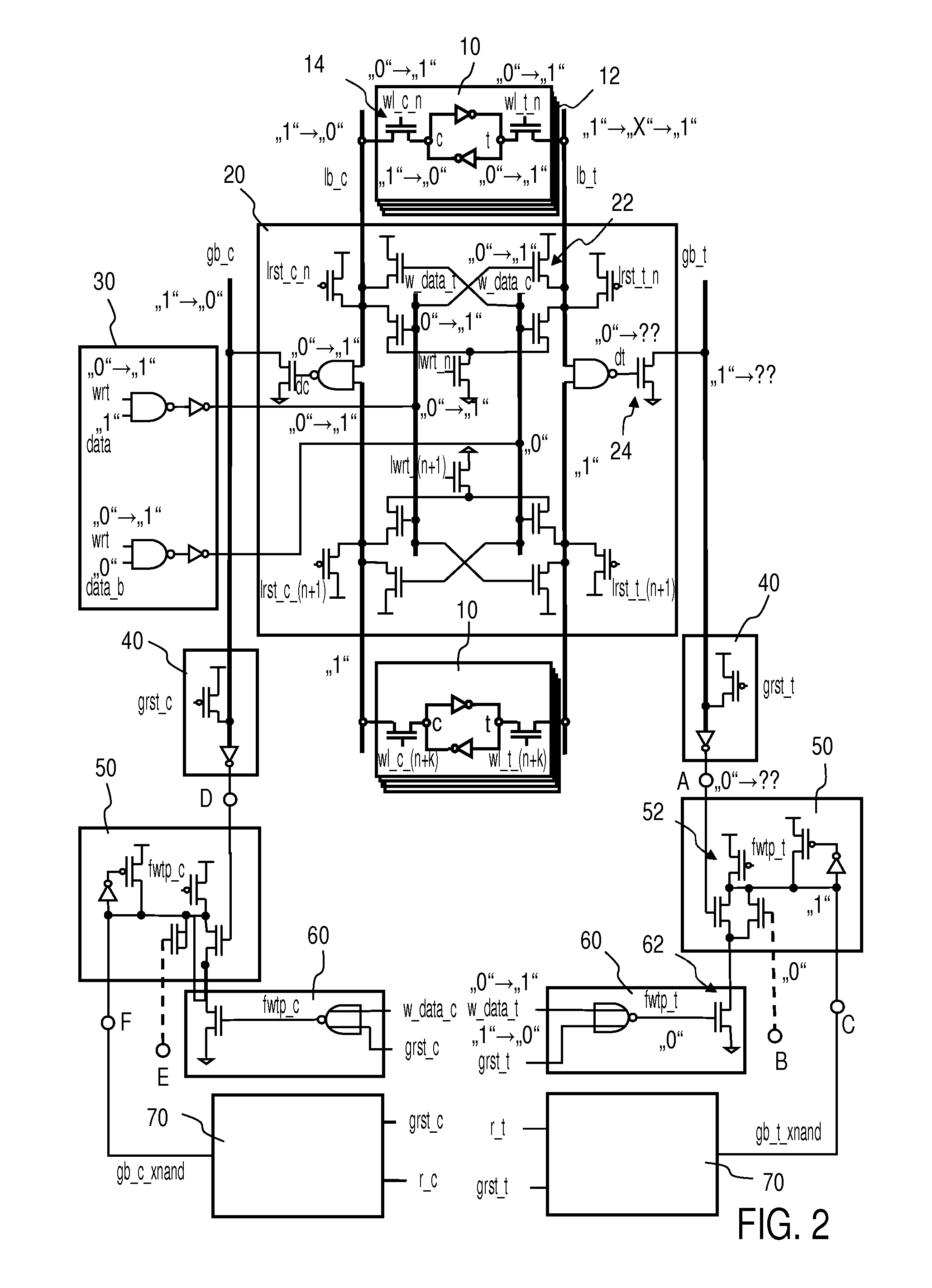
FIG. 1 is a schematic block diagram of a SRAM array 1 with write through capability, in accordance with an embodiment of the present invention, and FIG. 2 is a schematic circuit diagram of an upper part of the SRAM array 1 shown inFIG. 1, in accordance with an embodiment of the present invention. For the sake of simplicity, only the upper part of the SRAM array 1 is shown in detail herein.

Referring to FIGS. 1 and 2, the shown embodiment of the present invention employs a SRAM array 1 with write through capability comprising a plurality of SRAM cells 10 and corresponding local evaluation circuits 20 with local bit lines lb_t, lb_c and word lines wl_c_n, wl_t_n, wl_c_(n+k), wl_t_(n+k) for performing write and read operations, a write data gating logic 30 for generating dynamic write data w_data_t, w_data_c by combining input data data, data_b with a dynamic write enable signal wrt, read head circuits 40 to read logical level of global bit lines gb_t, gb_c, and a connecting structure 5...


PUM


Abstract

An improved method for performing a write through operation during a write operation of a SRAM cell (10) of a SRAM array (1) is disclosed. The method comprises suppressing a false write through data propagation at an output node (C, F) of the SRAM array (1) in case of a failure causing transition at a first node (t) or a second node (c) of the SRAM cell (10) by using information about the input data (data, data_b) to be written in the SRAM cell (10) and read data propagation paths to retain the output node (C, F) after a global bit line (gb_t, gb_c) at a precharge level independently from a logical level of the global bit line (gb_t, gb_c), if a corresponding node (c, t) of the SRAM cell (10) is performing the failure causing transition based on input data (data, data_b) to be written in the SRAM cell (10).

Description

BACKGROUND OF THE INVENTION1. Field of the InventionThe present invention relates in general to the field of digital memory circuits, and in particular to a method for performing a write through operation, and a circuit arrangement for performing a write through operation. Still more particularly, the present invention relates to a Static Random Access Memory (SRAM) array with write through capability.2. Description of the Related ArtStatic random access memory (SRAM) is a type of volatile digital memory that retains data written to it so long as power is applied to the SRAM. One type of SRAM commonly used in high performance computational circuits is referred to as a “domino” SRAM. A domino SRAM can have write-though capability that allows a value being written into the SRAM to be read at the output of the SRAM in the same cycle that the value is being written. This feature is useful while performing memory and logic self tests.When testing integrated circuits, techniques such as A...

Claims


Application Information

Patent Timeline
Patent Type & Authority Applications(United States)
IPC IPC(8): G11C11/34G11C11/00
CPCG11C11/41G11C29/48G11C29/1201G11C11/419
Inventor CHAN, YUEN H.KUGEL, MICHAELPELELLA, ANTONIOWERNER, TOBIAS
Owner IBM CORP
Why Eureka
Try Eureka