System and method for debugging multiple field-programmable gate arrays

A gate array and on-site technology, applied in the field of multi-chip FPGA debugging system, can solve the problems of multi-storage resources, time-consuming, multi-pins, etc., and achieve the effects of improving efficiency, saving pins, and saving compilation times

Active Publication Date: 2015-04-22
INSPUR BEIJING ELECTRONICS INFORMATION IND
View PDF7 Cites 11 Cited by
  • Summary
  • Abstract
  • Description
  • Claims
  • Application Information

AI Technical Summary

Problems solved by technology

Traditional embedded in-circuit logic analyzers are often incapable of doing this
At the same time, the embedded logic analyzer will occupy more storage resources. When the FPGA resource utilization rate is higher than 80%, inserting the embedded logic analyzer will also have a great adverse effect on FPGA layout and routing.
In addition, every time the captured signal of the online logic analyzer is updated, the entire design needs to be recompiled, which takes a long time
Using an external logic analyzer tends to occupy more pins, especially for scenarios where the observed signal bit width is wide. This problem is especially obvious.

Method used


Image

  • System and method for debugging multiple field-programmable gate arrays
  • System and method for debugging multiple field-programmable gate arrays
  • System and method for debugging multiple field-programmable gate arrays

Examples


Embodiment Construction

[0040] The technical solutions of the present invention will be described in detail below with reference to the accompanying drawings and preferred embodiments. It should be understood that the following examples are only used to illustrate and explain the present invention, but not to limit the technical solution of the present invention.

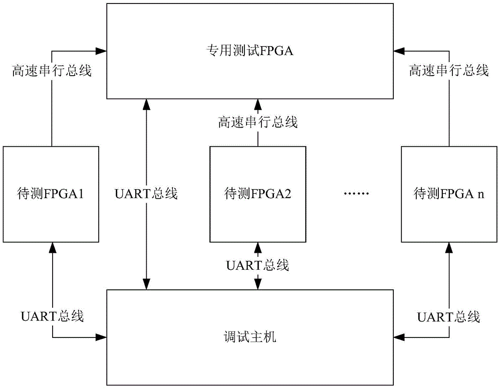
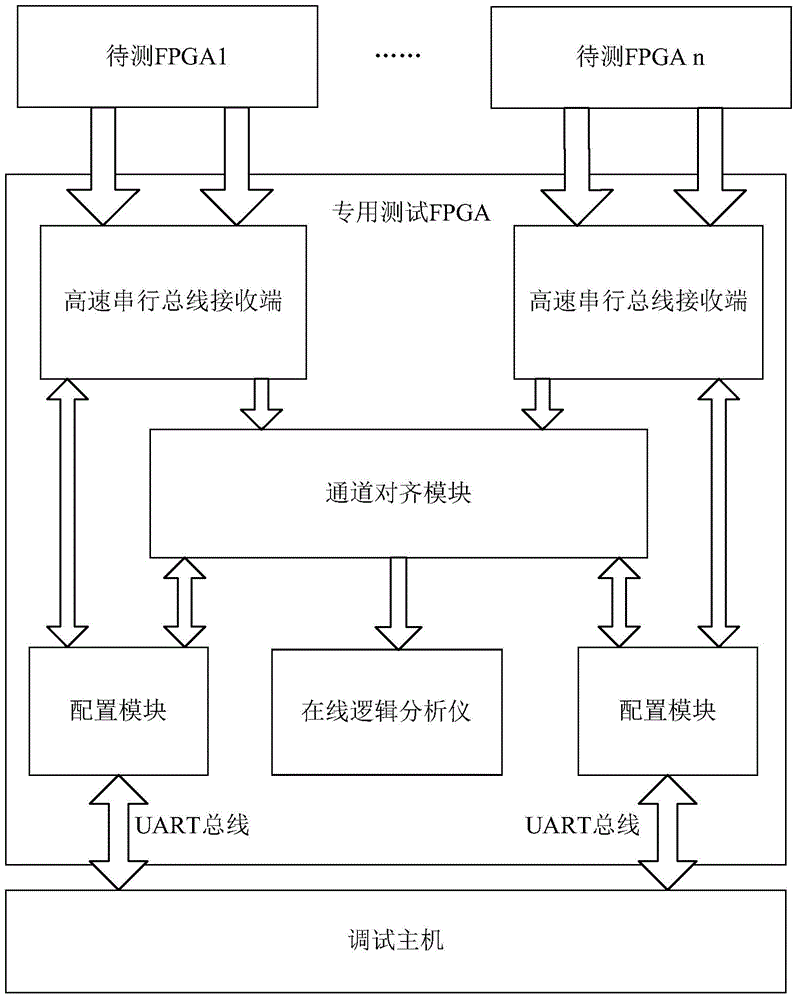
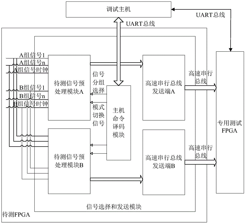
[0041] Such as figure 1 Shown, represented the structure of the system embodiment of multi-chip FPGA debugging of the present invention, including a special-purpose test FPGA, multi-chip FPGA to be tested and debugging host, wherein:

[0042]The FPGA to be tested is connected to a dedicated test FPGA through a high-speed serial bus, and connected to a debugging host through a serial bus, which is used to instantiate the signal selection and transmission modules of this chip to select and group the signals to be tested according to the clock domain; In the test working mode, according to the selection of the debugging host, the signal grou...


PUM


Abstract

The invention provides a system and a method for debugging multiple field-programmable gate arrays (FPGAs). The method comprises the following steps: selecting and grouping to-be-tested signals according to a clock domain by virtue of a signal selection and transmission module for instantiating each to-be-tested FPGA, and configuring a high-speed serial transceiver bus port of signal transmission; performing logic synthesis and location wiring on the design logic of the to-be-tested FPGAs and the signal selection and transmission module together; finding displacement information aligned with all channels according to the longest time delay in high-speed serial bus channels of all the to-be-tested FPGAs by using a special tested FPGA in a channel alignment operating mode selected by a debugging host; and selecting a to-be-tested signal group of the to-be-tested FPGA by the debugging host, and configuring the channel time delay value by using frequency information of the to-be-tested signal group. According to the system and the method disclosed by the invention, the cross-FPGA chip signal is observed and captured by using a special tested FPGA, and the fault tracing and positioning efficiency of a debugging system is improved.

Description

technical field [0001] The invention relates to a field programmable gate array (FPGA, Field Programmable Gate Array) debugging technology, in particular to a system and method for realizing multi-chip FPGA debugging. Background technique [0002] In recent years, the scope of large-scale FPGA applications has become wider and wider, and the application scenarios have become increasingly complex. Taking IC prototype verification as an example, IC design at the level of tens of millions of gates usually needs to be implemented with multi-chip (ie, multi-chip) FPGAs. In this way, it is necessary to jointly debug multiple FPGAs. The latter has always been a difficult problem in FPGA debugging. [0003] At present, the common solution is to build an embedded logic analyzer in each FPGA. Because these logic analyzers are logically divided into different FPGA slices, there is no physical connection between them, so it is impossible to use the signal of one FPGA as a trigger sig...

Claims


Application Information

Patent Timeline
Patent Type & Authority Applications(China)
IPC IPC(8): G06F11/26
Inventor 岳自超
Owner INSPUR BEIJING ELECTRONICS INFORMATION IND
Why Eureka
Try Eureka