NAND FLASH system and controller, as well as data processing method of controller

A controller and data technology, applied in the direction of instruments, static memory, read-only memory, etc., can solve the problems of increasing the communication difficulty of electronic equipment, unfavorable mobile phones, increasing the volume of electronic equipment, etc.

Inactive Publication Date: 2015-12-30
GIGADEVICE SEMICON (BEIJING) INC
View PDF3 Cites 0 Cited by
  • Summary
  • Abstract
  • Description
  • Claims
  • Application Information

AI Technical Summary

Problems solved by technology

However, limited by the width of address bits and data bits, NANDFLASH usually has a lot of pins, such as only IOx may occupy 8 or 16 pins, and because NANDFLASH bare chips generally need to be integrated in electronic equipment, this not only increases It increases the difficulty of communication with electronic devices and increases the volume of electronic devices. Therefore, it is not conducive to mobile phones and other electronic devices that have special requirements for volume.

Method used


Image

  • NAND FLASH system and controller, as well as data processing method of controller
  • NAND FLASH system and controller, as well as data processing method of controller
  • NAND FLASH system and controller, as well as data processing method of controller

Examples


Embodiment Construction

[0035] In order to make the above objects, features and advantages of the present invention more comprehensible, the present invention will be further described in detail below in conjunction with the accompanying drawings and specific embodiments.

[0036] System embodiment

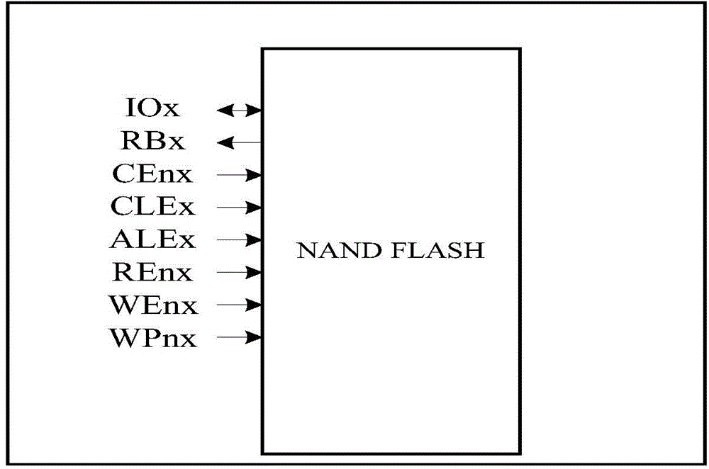
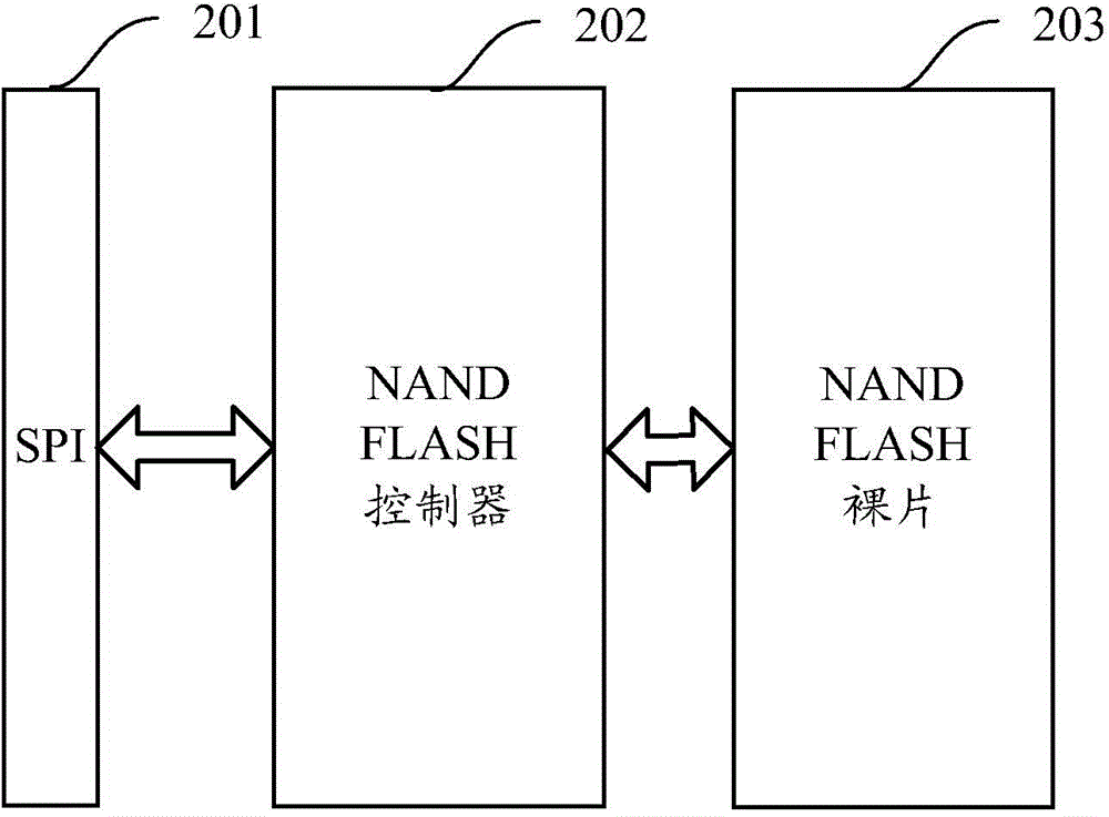
[0037] refer to figure 2 , shows a structural block diagram of a NANDFLASH system embodiment of the present invention, which may specifically include: serial peripheral interface (SPI, SerialPeripheralInterface) 201, NANDFLASH controller 202 and NANDFLASH bare chip 203 connected in sequence;

[0038] Wherein, the NANDFLASH controller 202 is connected to the SPI201 through a serial port, and is connected to the NANDFLASH die 203 package through a parallel port, and is used to convert the first parallel data input by the NANDFLASH die 203 into a first serial The data is output through the SPI201, and the second serial data input by the SPI201 is converted into second parallel data and output to the NANDF...


PUM


Abstract

The invention provides a NAND FLASH system, a NAND FLASH controller and a data processing method of the NAND FLASH controller. The NAND FLASH system comprises a serial peripheral interface (SPI), the NAND FLASH controller, and a NAND FLASH bare chip, wherein the NAND FLASH controller is connected with the SPI through a serial port, connected with the NAND FLASH bare chip through a parallel port, and used for converting first parallel data inputted by the NAND FLASH bare chip into first serial data and outputting the first serial data through the SPI, as well as converting second serial data inputted by the SPI into second parallel data and outputting the second parallel data to the NAND FLASH bare chip. Through adoption of the NAND FLASH system, the NAND FLASH controller and the data processing method, the difficulty in communication between the NAND FLASH bare chip and electronic equipment as well as the volume occupied by the NAND FLASH bare chip can be reduced.

Description

technical field [0001] The invention relates to the technical field of semiconductor memory, in particular to a NAND FLASH system, a NAND FLASH controller and a data processing method thereof. Background technique [0002] NAND flash memory (NAND FLASH Memory) is a non-volatile memory that can be electrically erased online. It has the advantages of fast erase and write speed, low power consumption, large capacity, and low cost. It is widely used in MP3, MP4, mobile phones, digital cameras, Cameras, security equipment and other electronic equipment [0003] Existing NANDFLASH dies usually use a parallel interface, for example, refer to figure 1 , shows an example of an existing parallel interface of NANDFLASH, wherein, IOx is the data IO interface for NANDFLASH to communicate with the outside world, RBx is the current state identification signal of NANDFLASH, CEnx is the chip select signal of NANDFLASH, and CLEx is the receiving command lock of NANDFLASH Deposit signal, ALE...

Claims


Application Information

Patent Timeline
Patent Type & Authority Applications(China)
IPC IPC(8): G11C16/06G11C29/42
Inventor 刘会娟苏志强张君宇
Owner GIGADEVICE SEMICON (BEIJING) INC
Why Eureka
Try Eureka