Single-crystalline film and process for production thereof

a single-crystalline film and film technology, applied in the direction of polycrystalline material growth, instruments, transportation and packaging, etc., can solve the problems of difficult preparation of uniform films, failure to provide single-crystalline films, and difficult to obtain single-crystalline thin films

Inactive Publication Date: 2004-04-22
CANON KK
View PDF12 Cites 2 Cited by
  • Summary
  • Abstract
  • Description
  • Claims
  • Application Information

AI Technical Summary

Problems solved by technology

According to any of such processes, however, it is difficult to obtain a thin film of single crystal by suppressing the thickness increase, and this poses an obstacle against using it as a functional layer in devices which have a laminar structure in many cases.
As another process, there is known a gas phase deposition process, by which, however, it is difficult to prepare a uniform film due to affection by the gas phase deposition boundary.
As a result of my study, however, such a crystal film obtained through the above-described process in general can only form a poly-crystalline film and fails to provide a single-crystalline film.

Method used


Image

  • Single-crystalline film and process for production thereof
  • Single-crystalline film and process for production thereof
  • Single-crystalline film and process for production thereof

Examples


example 1

[0047] A cell having a layer structure schematically illustrated in FIG. 1 was prepared.

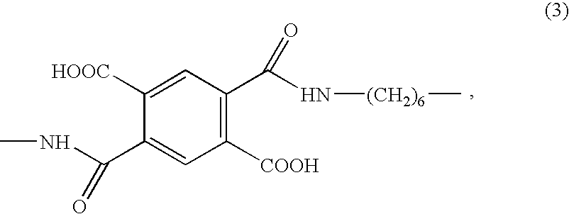
[0048] Two glass sheets each having a thickness of 1.1 mm and an areal size of ca. 20 mm.times.20 mm were respectively coated with a 700 .ANG.-thick ITO transparent conductor film by sputtering and further with a 0.7 wt. % solution in NMP (N-methylpyrrolidone) of a polyamic acid ("LP-64", made by Toray K. K.) having a recurring unit of formula (3) below by spin coating at 2000 rpm for 20 sec: 2

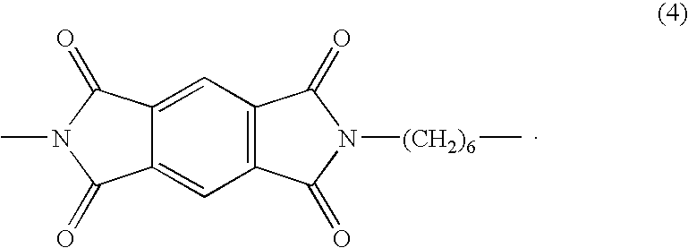
[0049] followed by pre-drying at 80.degree. C. for 5 min. and baking at 200.degree. C. for 60 min. to form a 50 .ANG.-thick film of polyimide represented by formula (4) below: 3

[0050] The polyimide film on each glass substrate was subjected to four times of rubbing in one direction with a nylon-planted cloth at a roller feed speed of 10 mm / sec and a roller revolution speed of 1000 rpm.

[0051] The two substrates treated in the above-described manner were applied to each other with 2.4 .mu.m-dia. spacer beads ...

example 1a

[0054] In order to examine the crystalline order of the respective regions in the crystalline film obtained in Example 1, a cell for X-ray diffraction analysis was prepared in the same manner as in Example 1 except for using 80 .mu.m-thick glass substrates.

[0055] The cell was set in a rotary pair cathode-type X-ray diffraction apparatus ("RU-300", made by Rigaku Denki K. K.) having an organization as illustrated in FIG. 10 to obtain X-ray diffraction patterns for the single crystal region (s-crystal) and poly-crystal region (p-crystal) respectively in FIG. 6 by a transmission method under the following conditions:

[0056] X-ray source: CuKa, 40 kV, 200 mA

[0057] Measurement conditions:

[0058] Effective line focus width=0.05 mm S1=0.15 mm, S2=SS2 deg., S3=0.3 mm,

[0059] Ni filter

[0060] Focus-S1=95 mm, S1-Sample=90 mm,

[0061] Sample-S2=143 mm, S2-S3=42 mm

[0062] Incident angle (.alpha. deg.)=fixed

[0063] 2.theta.-scan 1 deg. / min., Interval=0.02 deg.

[0064] Angle resolution=ca. 3.5 rad (=ca. 0....

example 2

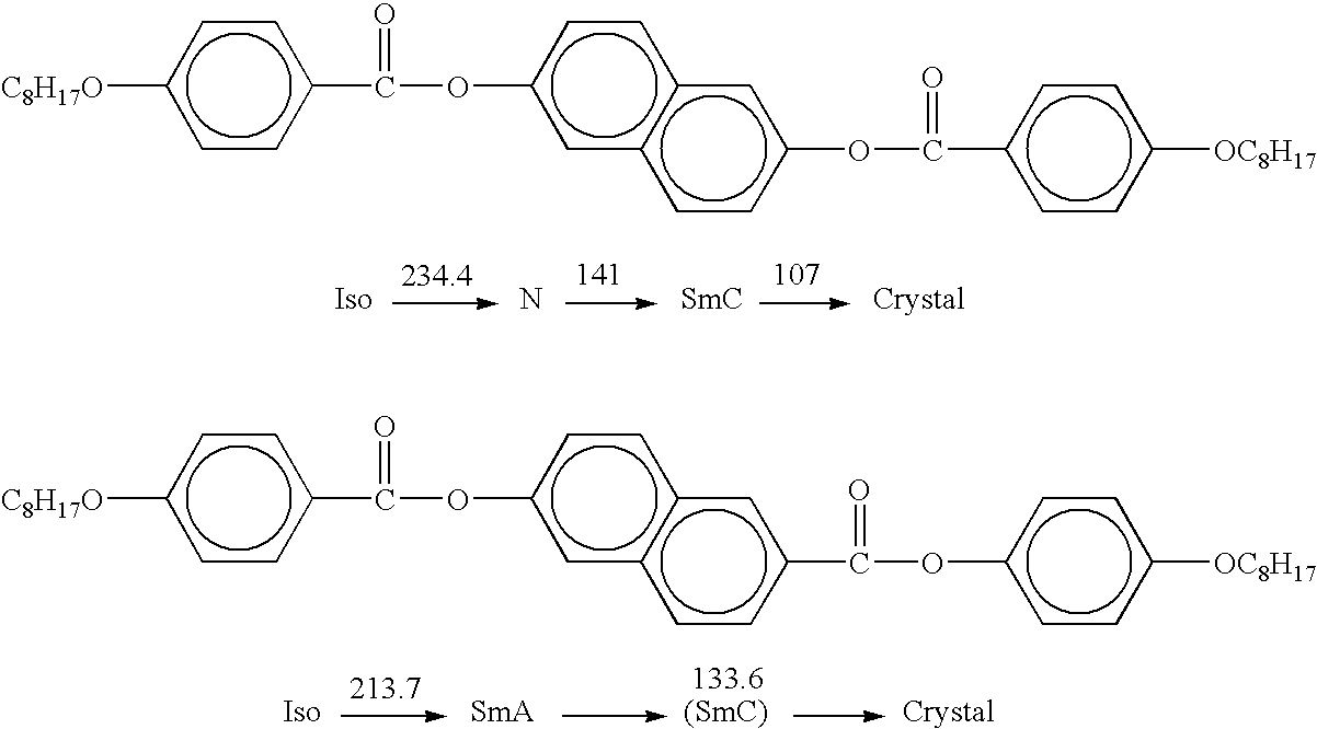
[0068] The cell prepared in Example 1 was again heated to a nematic phase temperature (130.degree. C.) and thereafter started to be cooled at a rate of 1.degree. C. / min. similarly as in Example 1. In this Example, however, the cell was not continually cooled to room temperature as in Example 1 but held for 30 min. at 118.degree. C. which was a crystal phase temperature lower than the SmC-Crystal transition temperature (=122.degree. C.) and thereafter cooled to room temperature. In the meantime, the alignment states were photographed through a polarizing microscope after holding for 1 min. and 10 min., respectively, at 118.degree. C. The thus-obtained photographs (each in a magnification of 100) are attached hereto as FIGS. 7 and 8, respectively.

[0069] With the lapse of time of the holding at 118.degree. C., the single crystal region was remarkably enlarged to ca. 80% of the cell area (20 mm.times.20 mm) as shown in FIG. 7 after holding for 1 min., which already exceeded the single c...


PUM

PropertyMeasurementUnit
thicknessaaaaaaaaaa
transition temperatureaaaaaaaaaa

Abstract

An organic single-crystalline film usable as a functional film in various devices is produced by selecting a liquid crystal material having a good molecular alignment regularity, disposing the liquid crystal material between a pair of boundaries exerting a thickness regulating force and solidifying the liquid crystal material while imparting a molecular alignment order by phase transition from a liquid crystal phase. The liquid crystal material may preferably be a smectic liquid crystal material which provides a uniform molecular alignment inclusive of the direction of molecular long axis in a smectic phase.

Description

FIELD OF THE INVENTION AND RELATED ART[0001] The present invention relates to a molecular single-crystalline film (which herein refers to a film having a thickness of at most ca. 100 .mu.m and having a portion which retains a single crystal state having a uniform molecular crystalline alignment over the thickness and over an areal extension including a side length of at least 10 times the thickness, i.e., an areal size utilizable as a functional film, preferably an areal size of at least 50 .mu.m.times.50 .mu.m), and a process for production thereof.[0002] A molecular crystal can be expected as a useful device material, such as a superconducting material, an effective photoconductor or a gas sensor, because of its electronical and geometrical structure and packing state. As the process for production thereof, growth in a solution and growth in a molten state have been generally practiced. According to any of such processes, however, it is difficult to obtain a thin film of single cr...

Claims


Application Information

Patent Timeline
Patent Type & Authority Applications(United States)
IPC IPC(8): G02F1/13C09K19/02C09K19/32C30B9/04C30B29/54
CPCC09K19/02C09K19/0403C09K19/2007Y10T428/10C09K19/322C09K2019/0444Y10T428/1036C09K19/32C09K2323/00C09K2323/03
Inventor HANYU, YUKIO
Owner CANON KK
Why Eureka
Try Eureka