

Plastic male mold for fabricating microstructures and nanostructures using imprint lithography
a technology of imprint lithography and molds, which is applied in the field of plastic male molds for fabricating microstructures and nanostructures using imprint lithography, can solve the problems of nano-scale resist structures, nano-scale resist structures, and electron beam lithography is used only for fabricating molds,
Inactive Publication Date: 2004-04-29
MICRO RESIST TECH
View PDF2 Cites 11 Cited by
- Summary
- Abstract
- Description
- Claims
- Application Information
AI Technical Summary
Benefits of technology
"The invention describes a method for making molds for micro and nanostructures using a negative system of lithographically fabricated structures. The method involves using photo-reactive epoxy resins that are sensitive to high-energy radiation and have good thermal stability. The process involves fabricating a master structure using electron beam lithography, and then embossing the structure into a coated material. The embossed structure can then be used as a mold for further embossing. The invention solves the problem of using time-consuming and cost-intensive electron beam resins and plasma etching for transferring the mold structure to other materials. The method allows for the fabrication of molds with high precision and resolution."
Problems solved by technology
In this context, cost-intensive and time consuming electron beam lithography is used only for fabricating the mold.
The properties of the electron beam resists hitherto available do not, however, permit their direct use as molds.
The structure transfer of nano-scaled resist structures to more stable inorganic materials poses a number of problems.
The plasma etching resistance of conventional hyper-sensitive electron beam resists is insufficient, and their galvanic copying process places special demands on the profile of the structure, and on the thermal stability and solubility of the resist structures (Introduction to Microlithography; L. E. Thompson et al., ACS Professional Reference Book, American Chemical Society, Washington D.C., 1994).
This may usually be realized by combinations of different polymers or by using special auxiliary layers in multiple-layer systems and necessitates further partial steps and, therefore, a loss of precision and resolution of the structures.
Method used
View moreImage
Smart ImageViewing Examples

Examples
example 2
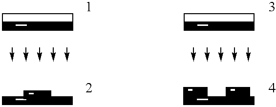
[0012] The resist structure fabricated in example 1 and its copy were used in nano imprint lithography for embossing the structure (table). Compared to a SiO.sub.2--mold no differences in quality resulted in copying the structure.
Login to View More PUM
| Property | Measurement | Unit |
|---|---|---|
| thicknesses | aaaaa | aaaaa |
| temperature | aaaaa | aaaaa |
| temperature | aaaaa | aaaaa |
Abstract
Known electron beam lithography used for manufacturing male molds is cost-intensive and very time consuming. As a result, conventional highly sensitive electron beam resists have an insufficient plasma etching resistance and galvanic molding makes special demands on the structural profile and the thermal stability and solubility of the resist structures. The novel production and use of lithographically produced resist structures as male mold material for use in imprint lithography for producing microstructures and nanostructures should thus overcome the drawbacks associated with the conventional procedure for producing male molds. To this end, a negative resist system is used whose lithographically produced structures correspond to the demands made on a male mold for molding thin polymer layers. Lithographically produced structures comprised of curable materials are thus used for molding, preferably those based on photo-reactive epoxy resins. The invention, in turn, enables an economical and thereby low-cost production of male mold material.
Description
[0001] The invention describes the fabrication and use of lithographically produced resist structures used as mold material for imprint lithography for fabricating micro and nanostructures.THE STATE OF THE ART[0002] Structures dimensioned on the nanometer scale may be economically fabricated in large numbers by imprint lithography. (S. Y. Chou et al. Vac. Sci. Technol. B 15(6) (1997), 2897; U.S. Pat. No. 5,772,905). In this context, cost-intensive and time consuming electron beam lithography is used only for fabricating the mold. A large number of imprints may then be produced with the fabricated molds by thermal embossing of layers of polymeric materials on different substrates. The properties of the electron beam resists hitherto available do not, however, permit their direct use as molds. Following its development process, the structural layout imprinted directly on the resist layers must be transferred to more stable materials by several partial steps, such as plasma etching and...
Claims
Login to View More Application Information
Patent Timeline
 Patent Type & AuthorityApplications(United States)
IPC IPC(8): G03F7/00
CPCB82Y10/00G03F7/0017G03F7/0002B82Y40/00
InventorAHRENS, GISELGRUETZNER, GABIPFEIFFER, KARLREUTHER, FREIMUTH
OwnerMICRO RESIST TECH