Piezoelectric thin film element, manufacturing method thereof, and liquid ejecting head and liquid ejecting apparatus employing same

a technology manufacturing method, which is applied in the direction of piezoelectric/electrostrictive device details, device details, inking apparatus, etc., can solve the problems of increasing the number of layers formed, reducing productivity, and risking the reliability of piezoelectric thin film elements

Inactive Publication Date: 2004-05-13
SEIKO EPSON CORP
View PDF7 Cites 32 Cited by
  • Summary
  • Abstract
  • Description
  • Claims
  • Application Information

AI Technical Summary

Problems solved by technology

However, using stacked material comprising a plurality of thin layers for the PZT crystal film has disadvantages in that the number of layers must be increased in order to obtain the desired thickness, increasing the number of processes for forming the layers and decreasing pr

Method used


Image

  • Piezoelectric thin film element, manufacturing method thereof, and liquid ejecting head and liquid ejecting apparatus employing same
  • Piezoelectric thin film element, manufacturing method thereof, and liquid ejecting head and liquid ejecting apparatus employing same
  • Piezoelectric thin film element, manufacturing method thereof, and liquid ejecting head and liquid ejecting apparatus employing same

Examples


second embodiment

Manufacturing Method of Second Embodiment

[0098] Next, the method for manufacturing a piezoelectric element according to the second embodiment is described. FIGS. 9 and 10 are cross-sectional schematic views showing the method for manufacturing a piezoelectric element and a liquid ejecting head (inkjet recording head) of the second embodiment.

Step for Forming the Diaphragm (S1)

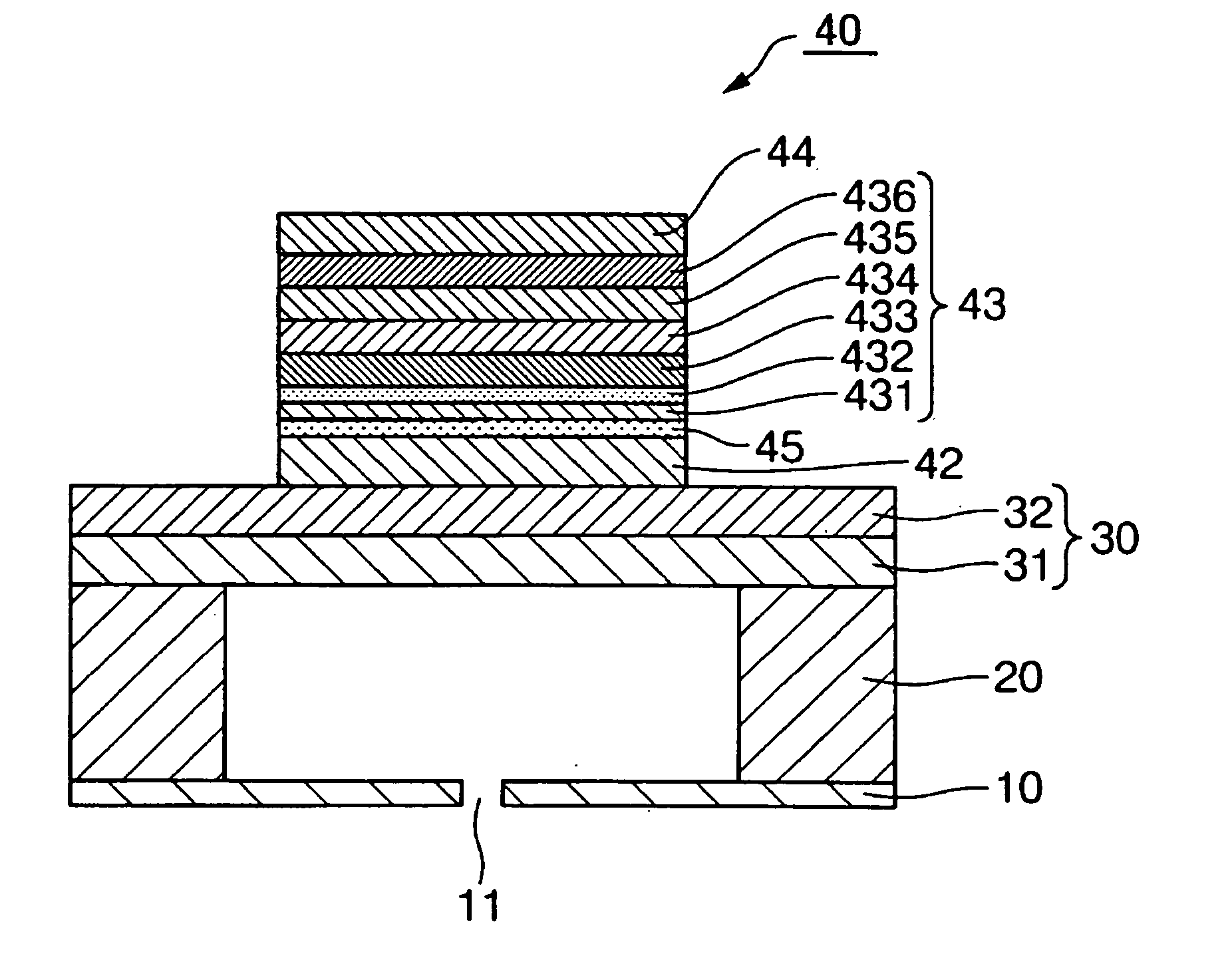
[0099] An insulating film 31 is formed on a silicon substrate that functions as the pressure chamber substrate 20. The thickness of the silicon substrate may, for example, be about 200 .mu.m. To manufacture the insulating film, a high-temperature treatment is performed in an oxidizing atmosphere containing water vapor or oxygen, yielding a silicon dioxide (SiO.sub.2) film with a thickness of, for example, 1 .mu.m. In addition to the commonly used thermal oxidation, CVD can also be used.

[0100] Furthermore, a ZrO.sub.2 film 32 with a thickness of 400 nm is formed on the insulating film 31. The ZrO.sub.2 film 32 i...


PUM

PropertyMeasurementUnit
Fractionaaaaaaaaaa
Thicknessaaaaaaaaaa
Thicknessaaaaaaaaaa

Abstract

The present invention provides a piezoelectric thin film element with superior piezoelectric properties in which the condition of the crystal of the piezoelectric thin film is appropriately controlled, and a manufacturing method thereof, as well as a inkjet recording head, inkjet printer, or other liquid ejecting apparatus employing the same. The piezoelectric thin film element 40 comprises a top electrode 44, a bottom electrode 42, and a piezoelectric thin film 43 formed between the top electrode 44 and the bottom electrode 42, wherein the piezoelectric thin film 43 is structured so as to comprise a first layer 431 located nearest to the bottom electrode and second layers (433-436) that are located nearer to the top electrode than the first layer and that each have a thickness greater than that of the first layer 431.

Description

[0001] 1. Field of the Invention[0002] The present invention relates to a piezoelectric thin film element, a manufacturing method thereof, and a liquid ejecting head and liquid ejecting apparatus employing the same, and more particularly to a piezoelectric thin film element or the like with superior piezoelectric properties and productivity.[0003] 2. Description of the Related Art[0004] Piezoelectric thin film elements that employ piezoelectric thin films that contain crystals typified by PZT (lead zirconate titanate; Pb(Zr.sub.xTi.sub.1-x)O.sub.3) have functions such as spontaneous polarization, high permittivity, electro-optic effects, piezoelectric effects, and pyroelectric effects, and are applied in extensive device development.[0005] A piezoelectric thin film element is structured by sequentially stacking a substrate, a diaphragm, a bottom electrode, a piezoelectric thin film, and a top electrode. Since piezoelectric properties of a piezoelectric thin film vary according to th...

Claims


Application Information

Patent Timeline
IPC IPC(8): B41J2/055B41J2/135B41J2/14B41J2/045B41J2/16H01L41/09H01L41/187H01L41/22H01L41/318H01L41/319H01L41/39
CPCB41J2/14233Y10T29/4913B41J2/1623B41J2/1628B41J2/1642B41J2/1645B41J2/1646B41J2002/14258B41J2002/14491B41J2202/03H01L41/29H01L41/318H01L41/0973H01L41/1876Y10T29/49128Y10T29/42Y10T29/49126Y10T29/49156B41J2/161H10N30/2047H10N30/8554H10N30/06H10N30/078
Inventor MURAI, MASAMI
Owner SEIKO EPSON CORP
Why Eureka
Try Eureka