Controlling data strobe output

a data strobe and output technology, applied in the field of semiconductor memory devices, can solve problems such as errors in accessing data stored in memory, information storage, static storage, etc., and achieve the effect of reducing the number of memory devices, and improving the quality of data storag

Inactive Publication Date: 2004-05-20
ROUND ROCK RES LLC
View PDF3 Cites 92 Cited by
  • Summary
  • Abstract
  • Description
  • Claims
  • Application Information

AI Technical Summary

Problems solved by technology

These devices are very densely packed, i.e., there is little space between them.
Errors occurring during the capturing of addresses and data may cause errors in accessing the data stored in memory.
Many of today's memory devices, such as double data rate RAM devices (DDR RAM), require intricate timing schemes for proper operation.
The memory devices may contain an inherent latency in the operation and reaction to commands and clock signals from external sources.
For example, there may be an inherent latency between the time tha...

Method used


Image

  • Controlling data strobe output
  • Controlling data strobe output
  • Controlling data strobe output

Examples


Embodiment Construction

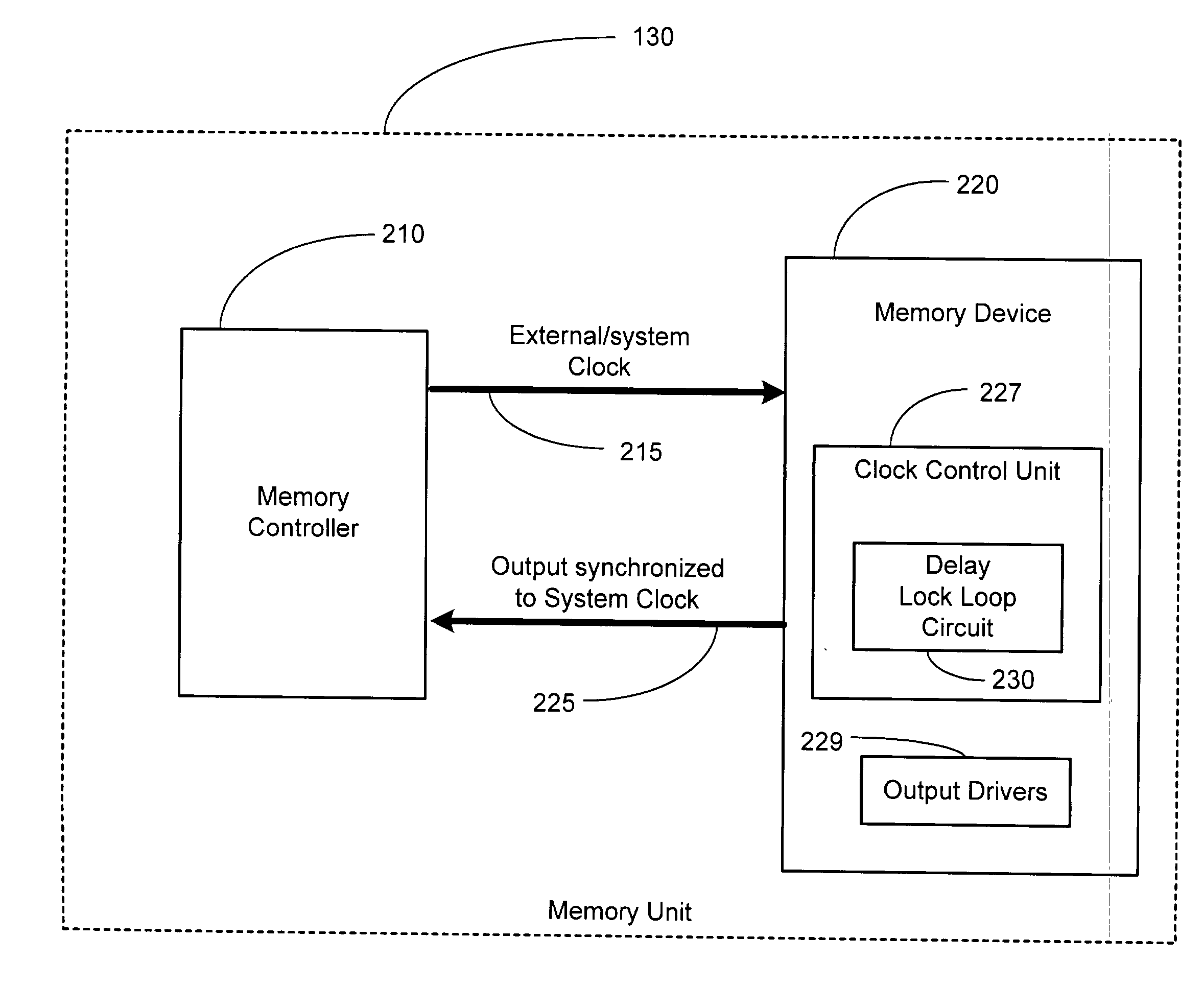
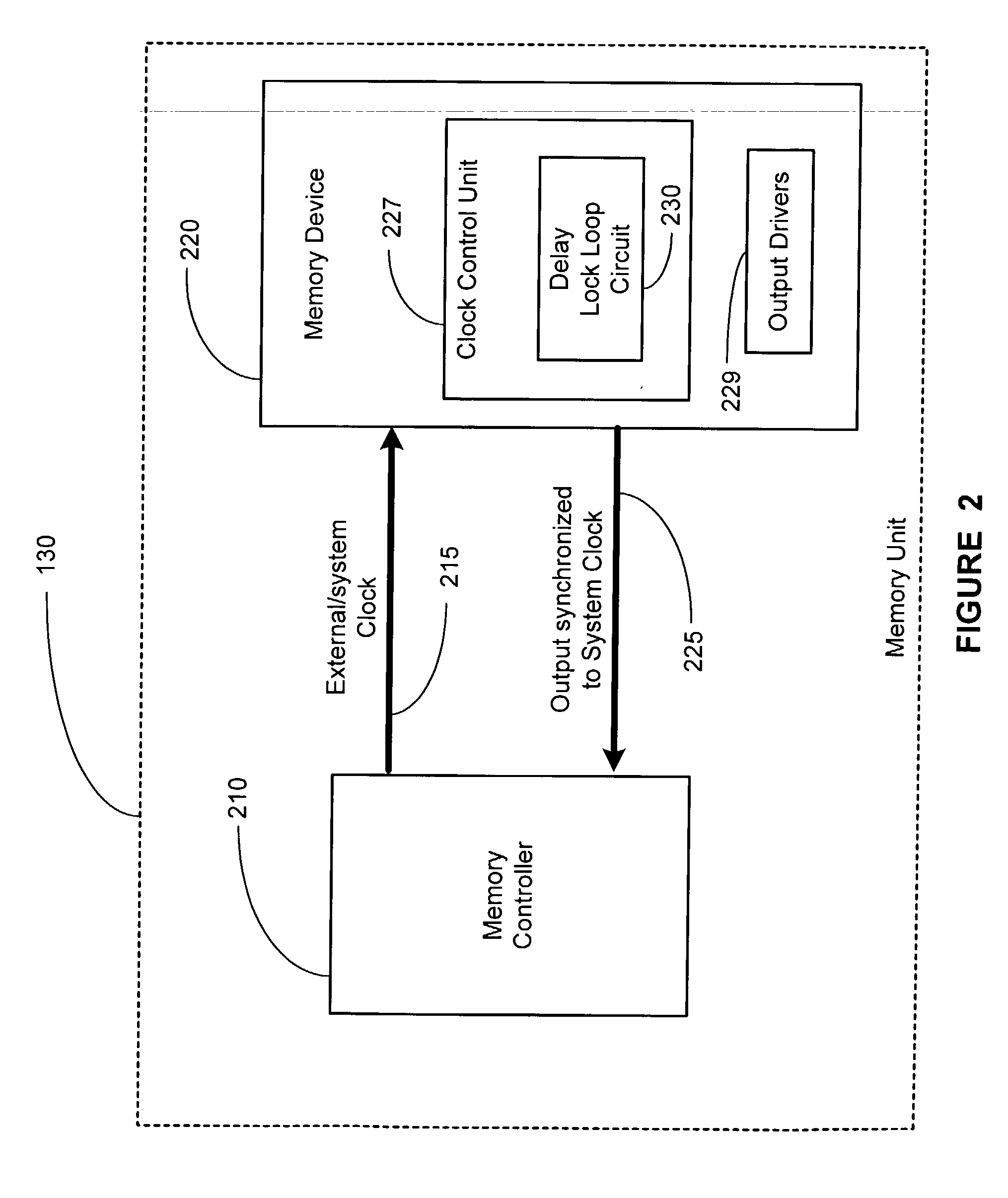
[0028] Illustrative embodiments of the invention are described below. In the interest of clarity, not all features of an actual implementation are described in this specification. It will of course be appreciated that in the development of any such actual embodiment, numerous implementation-specific decisions must be made to achieve the developers' specific goals, such as compliance with system-related and business-related constraints, which will vary from one implementation to another. Moreover, it will be appreciated that such a development effort might be complex and time-consuming, but would nevertheless be a routine undertaking for those of ordinary skill in the art having the benefit of this disclosure.

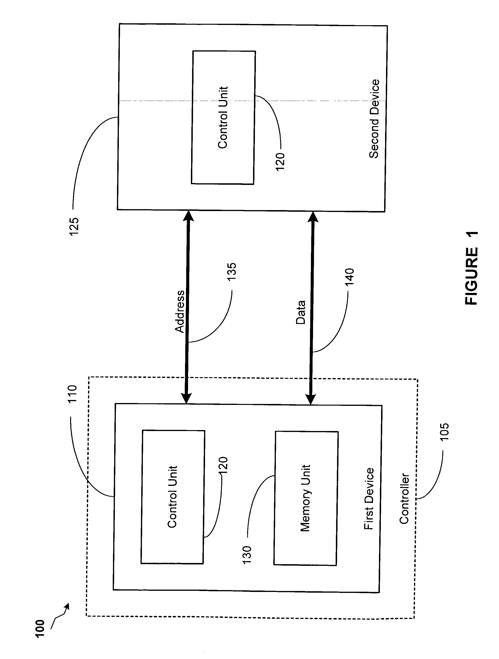
[0029] The timing of circuit operations is important for the proper operation of digital systems. Access of data / addresses, such as latching addresses and / or data, within precisely defined time periods is useful to ensure that data and / or addresses are properly captured by a dev...


PUM


Abstract

A method and apparatus is provided for controlling a data strobe. A latency of operation relating to a data operation of a device is determined. A delay lock loop signal is generated for the data operation of the device. The delay lock loop signal is compared to an external clock to determine a phase difference. A determination is made as to whether the delay lock loop signal is early based upon the phase difference. A signal is adjusted in response to the latency of operation is performed based upon the determination that the delay lock loop signal is early.

Description

[0001] 1. Field of the Invention[0002] This invention generally relates to semiconductor memory devices, and, in particular, to controlling a data strobe signal for accessing memory in a memory device.[0003] 2. Description of the Related Art[0004] Modern integrated circuit devices are comprised of millions of semiconductor devices, e.g., transistors, formed above a semiconductor substrate, such as silicon. These devices are very densely packed, i.e., there is little space between them. Similarly, densely packed electrically conducting lines may also be formed in the semiconductor substrate. By forming selected electrical connections between selected semiconductor devices and selected conducting lines, circuits capable of performing complex functions may be created. For example, bits of data may be stored by providing electrical current to a plurality of bit lines and an orthogonal plurality of wordlines that may be electrically coupled to one or more capacitors in a semiconductor me...

Claims


Application Information

Patent Timeline
IPC IPC(8): G11C7/10G11C7/22G11C11/4076G11C11/4096
CPCG11C7/1051G11C7/1066G11C11/4096G11C7/222G11C11/4076G11C7/22G11C7/04
Inventor LI, WEN
Owner ROUND ROCK RES LLC
Why Eureka
Try Eureka