NAND type flash EEPROM in which sequential programming process is performed by using different intermediate voltages

a technology of sequential programming and intermediate voltage, which is applied in the field of nand-type flash eeprom data programming system, can solve the problems of scaling and increasing the erroneous programming stress, and the programming stress decreases

Inactive Publication Date: 2004-06-03
KIOXIA CORP
View PDF4 Cites 36 Cited by
  • Summary
  • Abstract
  • Description
  • Claims
  • Application Information

AI Technical Summary

Problems solved by technology

However, the Vpass stress characteristic is the same as that in the SB system, but it is considered that the Vpgm stress becomes smaller than that in the SB system, and therefore, the intersection is shifted down to the left (erroneous programming stress decreases).
As the result of this, the scaling tends to increase the erroneous programming stress.
However, if the multi-value storage system is used, the threshold voltage range of the memory transistor used for data recording is enlarged, and therefore, it is inevitably necessary to enhance the program voltage Vpgm.

Method used


Image

  • NAND type flash EEPROM in which sequential programming process is performed by using different intermediate voltages
  • NAND type flash EEPROM in which sequential programming process is performed by using different intermediate voltages
  • NAND type flash EEPROM in which sequential programming process is performed by using different intermediate voltages

Examples


Embodiment Construction

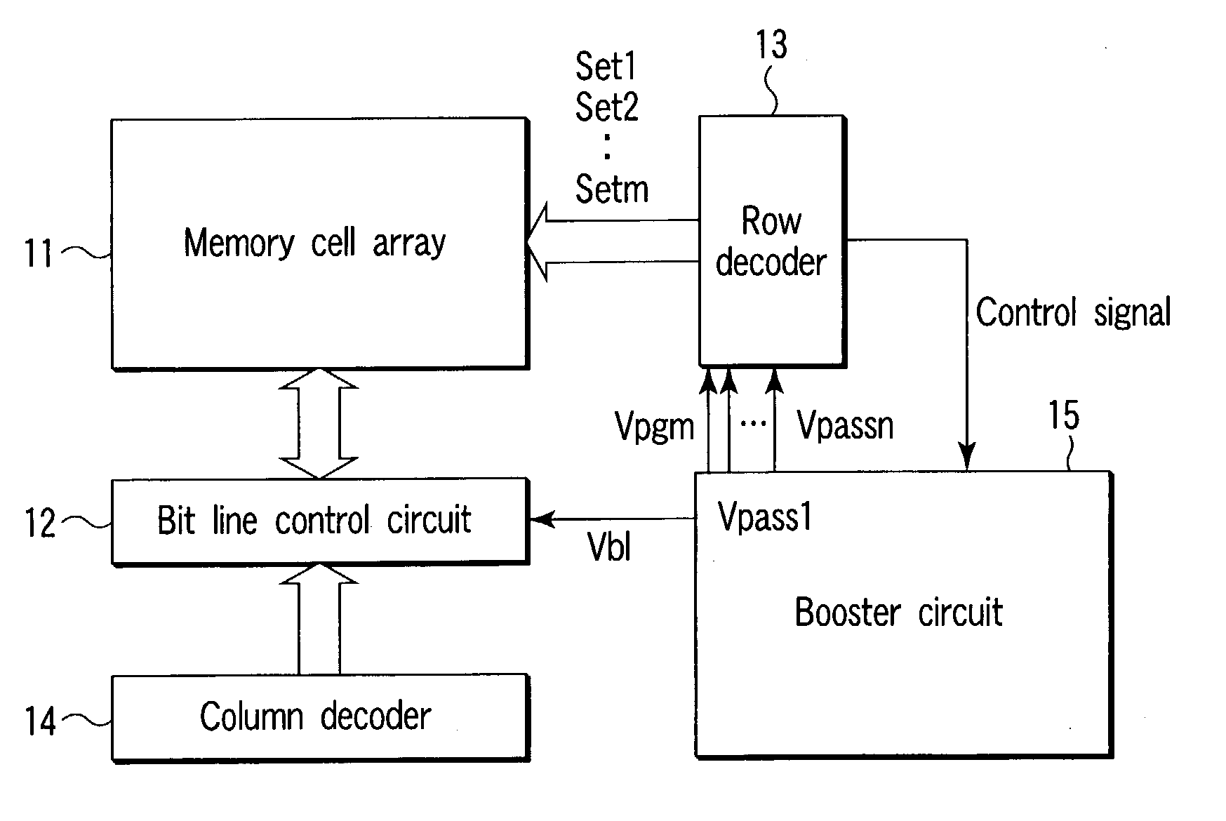
[0198] FIG. 27 is a block diagram showing an example of a memory card, for illustrating an application example of a nonvolatile semiconductor memory device according to an embodiment of the present invention.

[0199] As shown in FIG. 27, a memory chip (Flash memory) 92 used as a main memory and a controller chip (controller) 91 which controls the memory chip 92 are contained in a memory card 97. Only circuit blocks associated with the main memory among circuit blocks contained in the memory chip 91 are shown in FIG. 27 and explained with reference to FIG. 27.

[0200] As the circuit blocks associated with the main memory, for example, a serial / parallel and parallel / serial interface 93, page buffer 94 and memory interface 95 are provided.

[0201] For example, the interface 93 converts serial input data to parallel internal data when data is programmed into the memory chip 92. The converted parallel internal data is input to and stored in the page buffer 94. The stored internal data is suppl...


PUM


Abstract

A nonvolatile semiconductor memory device includes a NAND memory cell array, booster circuit, row decoder, bit line control circuit and column decoder. In the device, the magnitude of intermediate voltage applied to the control gates of memory transistors from the booster circuit via the row decoder is changed according to the position of a selected control gate line when data is sequentially programmed into the memory transistors in the memory cell array. Alternatively, a plurality of different intermediate voltages are applied when data is simultaneously programmed into memory transistors connected to the selected control gate line.

Description

[0001] This application is based upon and claims the benefit of priority from the prior Japanese Patent Application No. 2002-349199, filed Nov. 29, 2002, the entire contents of which are incorporated herein by reference.[0002] 1. Field of the Invention[0003] This invention relates to a nonvolatile semiconductor memory device, and more specifically, to a data programming system of a NAND type flash EEPROM, for example.[0004] 2. Description of the Related Art[0005] As a nonvolatile semiconductor memory device which can be electrically rewritten and formed with high integration density, a NAND type flash EEPROM is well known in the art. A memory transistor in the NAND type flash EEPROM has a stacked gate structure in which a charge storage layer (floating gate) and control gate are stacked and formed above a semiconductor substrate with an insulating film disposed therebetween. A NAND cell unit is configured by serially connecting a plurality of memory transistors in a column direction...

Claims


Application Information

Patent Timeline
Patent Type & Authority Applications(United States)
IPC IPC(8): G11C16/02G11C16/04G11C16/06G11C16/10H01L27/115
CPCG11C16/10G11C16/0483H10B69/00
Inventor MATSUNAGA, YASUHIKOYAEGASHI, TOSHITAKEARAI, FUMITAKA
Owner KIOXIA CORP
Why Eureka
Try Eureka