Scalable scan-path test point insertion technique

Inactive Publication Date: 2004-09-09
NEC CORP
View PDF1 Cites 26 Cited by
  • Summary
  • Abstract
  • Description
  • Claims
  • Application Information

AI Technical Summary

Benefits of technology

[0040] It will be significantly advantageous to overcome problems noted above and to enhance fault coverage for standard scan designs.
[0042] In a specific enhancement, the combinational test point is positioned to prevent shift dependency between the first standard scan cell and the second standard scan cell.
[0059] In another specific enhancement the combinational test point prevents shift dependency between the first standard scan cell and the second standard scan cell.
[0064] In another specific enhancement the combinational test point is positioned to prevent shift dependency between the first standard scan cell and the second standard scan cell.
[0066] Yet another aspect of the disclosed teachings is amethod for designing a circuit that is testable using a scan-based technique comprising accurately identifying, based on a functional analysis of the circuit, at least one pair of standard scan cells in the circuit where shift dependency occurs and inserting a test point at the identified point in the circuit.
[0085] In another specific enhancement when more than one backtrace is possible, a backtrace path that generates minimum controllability costs are used.

Problems solved by technology

However, developing functional test patterns that attain satisfactory fault coverage is unacceptable for large scale designs due to the prohibitive development cost.
Even if functional test patterns that can achieve high fault coverage are available, applying these test patterns at-speed for high speed chips requires very stringent timing accuracy, which can only be provided by very expensive automatic test equipments (ATEs).
A drawback of this method is performance degradation entailed due to additional logic that is inserted into the functional path.
Since this technique requires to replace all standard scan cells by enhanced scan cells, which can hold two bits, the drawback of enhanced scan testing is high area overhead of enhanced scan cells.
However, rearranging scan chains to enhance fault coverage may increase scan path routing overhead.
Furthermore, for circuits where most state inputs are topologically correlated, satisfactory transition delay fault coverage may not be achieved in any order of scan flip-flops.
Hence, the STR fault at line l is untestable by the skewed-load approach in standard scan environment.

Method used


Image

  • Scalable scan-path test point insertion technique
  • Scalable scan-path test point insertion technique
  • Scalable scan-path test point insertion technique

Examples


example

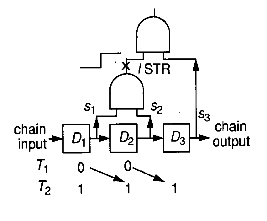
[0124] FIG. 5 illustrates calculating test point vectors for two example sets of test cube pairs: C.sup.1 and C.sup.2. Assume that adjacent pairs of state inputs, s.sub.2 and s.sub.3, s.sub.4 and s.sub.5, and s.sub.5 and s.sub.6, drive different fanout cones. Therefore, tp.sup.k.sub.3, tp.sup.k.sub.5, and tp.sup.k.sub.6, where k=1,2, are always assigned W's in every test point vector. When test cube pair V.sup.1 is added to C.sup.1, tp.sup.1.sub.2 is updated to O since s.sub.1 is assigned a 0 in V.sup.1.sub.1 and s.sub.2 is assigned a 1 in V.sup.1.sub.2, i.e., d.sup.1.sub.2=01, and tp.sup.1.sub.4 and tp.sup.1.sub.7 are updated to W0 since d.sup.1.sub.4=d.sup.1.sub.7=X0 in V.sup.1. When test cube pair V.sup.2 is added to C.sup.1, tp.sup.1.sub.4 is updated to A since d.sup.2.sub.4=10. On the other hand, tp.sup.1.sub.7 holds the previous value W0 since d.sup.2.sub.7=00. Assume that no test cube pair can be added to C.sup.1 without conflict after V.sup.2 is added. Now, all intermediate ...


PUM


Abstract

A logic circuit comprising at least one input, one output and a delay fault circuit. The delay fault circuit includes a first standard scan cell, a combinational test point positioned immediately after the first standard scan cell in a scan chain and a second standard scan cell positioned immediately after the combinational test point in the scan chain.

Description

I.A. RELATED APPLICATIONS[0001] This Application claims priority from co-pending U.S. Provisional Application Serial No. 60 / 447,272 filed Feb. 14, 2003, the contents of which are incorporated herein by reference.I.B. FIELD[0002] The present disclosure teaches techniques related to enhancing coverage of delay faults in scan designs for testing of circuits.I.C. BACKGROUND[0003] 1. References[0004] The following papers provide useful background information, for which they are incorporated herein by reference in their entirety, and are selectively referred to in the remainder of this disclosure by their accompanying reference numbers in square brackets (i.e., [3] for the third numbered paper by J. Monteiro and S. Devdas):[0005] [1] D. Belete, A. Razdan, W. Schwarz, R. Raina, C. Hawkins, and J. Morehead. Use of DFT Techniques In Speed Grading a 1 GHz+ Microprocessor. In Proceedings IEEE International Test Conference, pages 1111-1119, 2002.[0006] [2] K.-T. Cheng, S. Devadas, and K. Keutze...

Claims


Application Information

Patent Timeline
IPC IPC(8): G01R31/3183G01R31/3185
CPCG01R31/318328G01R31/318583G01R31/31858
Inventor WANG, SEONGMOONCHAKRADHAR, SRIMAT
Owner NEC CORP
Why Eureka
Try Eureka