Test circuit inserting method and apparatus for a semiconductor integrated circuit

a test circuit and integrated circuit technology, applied in error detection/correction, instruments, program control, etc., can solve the problems of increasing the chip size and the processing time for generating test patterns to achieve a desired fault coverage, so as to reduce the number of effective test points, increase the fault coverage of the entire chip, and reduce the effect of test points

Inactive Publication Date: 2007-04-17
SOCIONEXT INC
View PDF13 Cites 8 Cited by
  • Summary
  • Abstract
  • Description
  • Claims
  • Application Information

AI Technical Summary

Benefits of technology

[0010]An object of the present invention, to solve the above problem in the art, is to provide a test circuit inserting method and apparatus for a semiconductor integrated circuit which can reduce, for test point insertion points obtained by a conventional technique, the load of layout design that is performed after insertion of test circuits as well as can attain a high fault coverage while preventing increase in chip size.
[0011]To attain the above object, a test circuit inserting method for a semiconductor integrated circuit according to the invention comprises the steps of inputting circuit information; calculating controllability probabilities on the basis of the circuit information; performing initial layout on the basis of the circuit information; extracting interconnection pairs from a result of the initial layout; extracting test point insertion candidates on the basis of the controllability probabilities and the interconnection pairs; judging whether the test point insertion candidates exist; selecting test point insertion positions if the test point insertion candidates exist; selecting circuit structures of test points to be inserted at the test point insertion positions; virtually inserting the test points having the selected circuit structures; performing re-layout on a circuit in which the test points have been inserted virtually; judging whether circuit overhead of a result of the re-layout is within a prescribed range; and reducing the number of test points if the circuit overhead exceeds the prescribed range.
[0012]In the above-described method, causes of a low fault coverage are extracted by calculating 0-controllability probabilities and 1-controllability probabilities on the basis of the circuit information and interconnection pairs are extracted from layout information. The number of effective test points can be reduced by using those kinds of information. This makes it possible to reduce the load of layout design when test circuits are inserted at the test points and to attain a high fault coverage while preventing increase in chip size.

Problems solved by technology

However, with the increase in the circuit scale and the complexity of circuits, the processing time for generation of test patterns for attaining a desired fault coverage tends to increase.
However, in the above method, test points are merely determined on the basis of fault coverage and fault prevention information that are obtained by a fault simulation and the layout-related aspect of insertion of test circuits is not taken into account.
Therefore, the above method has a problem that wiring congestion is caused by insertion of test circuits, resulting in increase in chip size.

Method used


Image

  • Test circuit inserting method and apparatus for a semiconductor integrated circuit
  • Test circuit inserting method and apparatus for a semiconductor integrated circuit
  • Test circuit inserting method and apparatus for a semiconductor integrated circuit

Examples


first embodiment

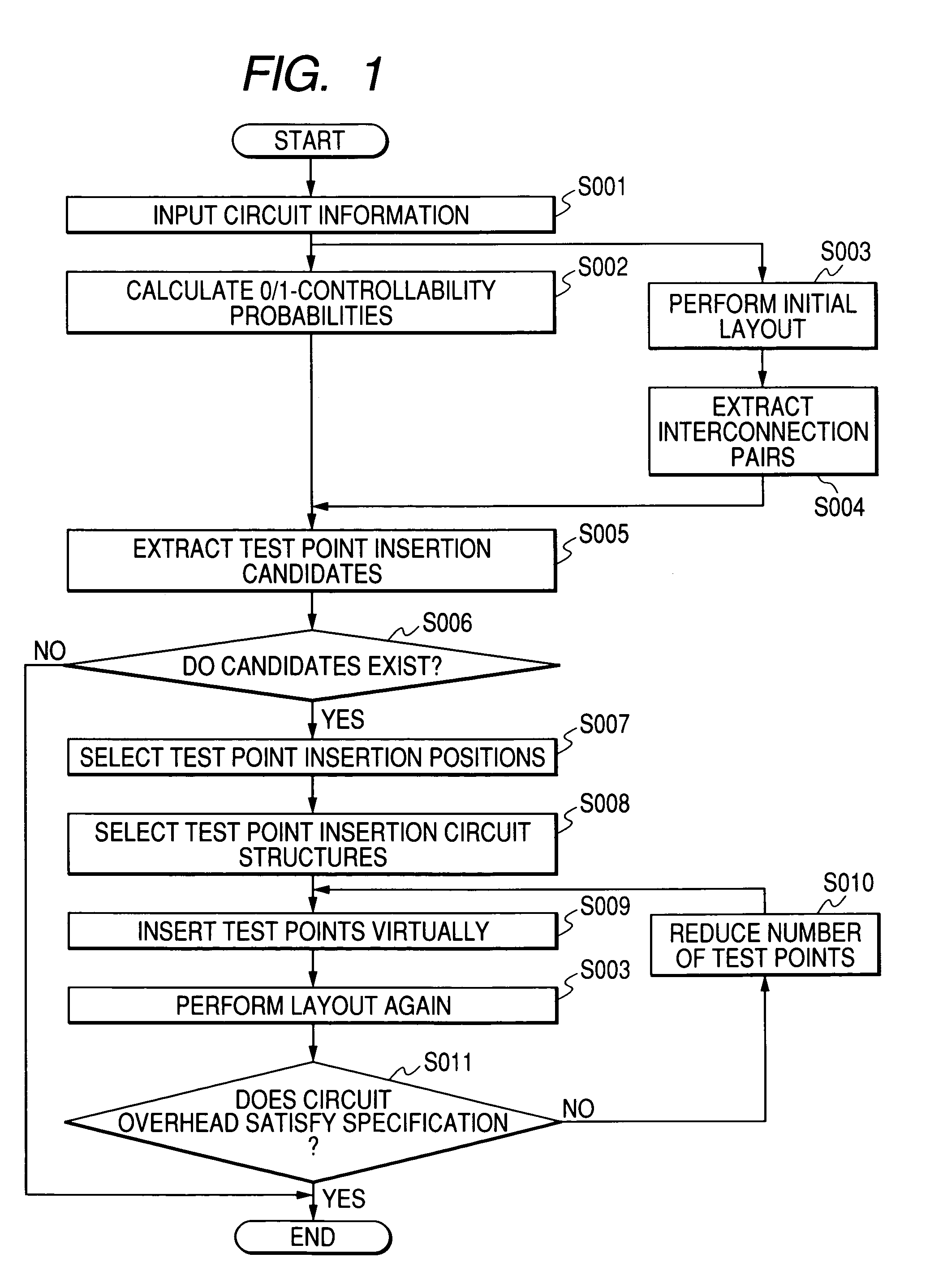
[0046]FIG. 1 is a flowchart of a process of a test circuit inserting method for a semiconductor integrated circuit according to a first embodiment of the present invention. As shown in FIG. 1, information of a subject circuit is input at step S001. At step S002, 0-controllability probabilities and 1-controllability probabilities are calculated for this circuit. Initial layout is performed on this circuit at step S003. At step S004, interconnection pairs where a problem may arise are extracted from a result of the initial layout.

[0047]Then, at step S005, test point insertion candidates are extracted by using the information obtained at steps S002 and S004. At step S006, it is checked whether the test point insertion candidates extracted at step S005 exist in terms of the configuration of the subject circuit. If it is judged as a result of the check that the candidates exist, test point insertion positions are selected at step S007 and test point insertion circuit structures are selec...

second embodiment

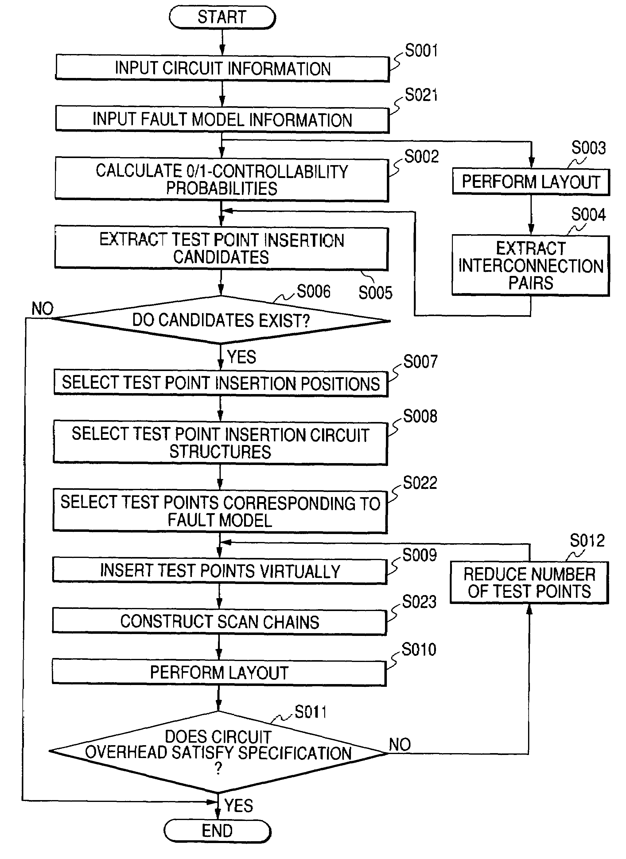
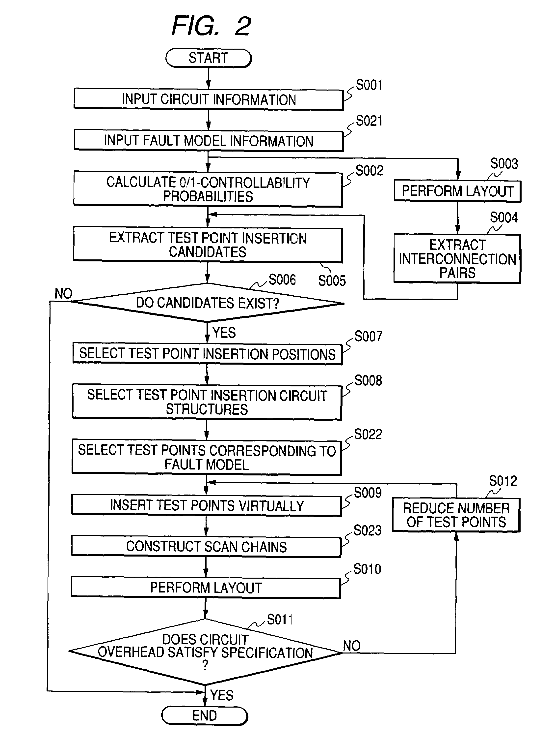
[0068]FIG. 2 is a flowchart of a process of a test circuit inserting method for a semiconductor integrated circuit according to a second embodiment of the invention. Steps in FIG. 2 having the same steps in FIG. 1 are given the same reference symbols as the latter and will not be described below.

[0069]In this embodiment, test points constitute scan chains. Further, to facilitate a defect analysis of a test result, fault model information is input in advance and the number of insertion positions of test points that are effective for the defect analysis is reduced in inserting test points. To this end, steps S021–S023 are added to the flowchart of FIG. 1.

[0070]As shown in FIG. 2, fault model information as a subject of analysis is input at step S021 immediately after circuit information is input at step S001. After circuit structures of test points to be inserted are selected by step S008 and the preceding steps, test points corresponding to the fault model that was set at step S021 a...


PUM


Abstract

A method to reduce the load of layout design and attain a high fault coverage while preventing increase in chip size in test point insertion for a semiconductor integrated circuit. Initial layout is performed on the basis of the circuit information. Interconnection pairs are extracted from a layout result. Test point insertion candidates are extracted on the basis of the controllability probabilities and the interconnection pairs. If test point insertion candidates exist, test point insertion positions are selected. Circuit structures of test points to be inserted there are selected. Test points having those circuit structures are inserted virtually. Whether the circuit overhead of a layout result is within a prescribed range is judged. If the circuit overhead exceeds the prescribed range, the number of test points is reduced.

Description

BACKGROUND OF THE INVENTION[0001]1. Field of the Invention[0002]The present invention relates to a design-for-testability technique for a semiconductor integrated circuit and, in particular, to a test circuit inserting method and a test circuit inserting apparatus.[0003]2. Description of the Related Art[0004]Design-for-testability techniques as typified by scan design are employed widely to attain a sufficiently high fault coverage in tests of semiconductor integrated circuits. However, with the increase in the circuit scale and the complexity of circuits, the processing time for generation of test patterns for attaining a desired fault coverage tends to increase. One countermeasure employed is a method of increasing the testability by inserting test points in a circuit.[0005]In a conventional test circuit inserting method for a semiconductor integrated circuit, a model circuit is configured on a computer in such a manner that logic elements and signal lines are arranged in the same...

Claims


Application Information

Patent Timeline
Patent Type & Authority Patents(United States)
IPC IPC(8): G06F17/50G01R31/28G06F11/00G01R31/3183H01L21/82
CPCG01R31/31835
Inventor SHIOTA, RYOJI
Owner SOCIONEXT INC
Why Eureka
Try Eureka