

Flash memory apparatus and method for merging data stored in the same
- Summary
- Abstract
- Description
- Claims
- Application Information
AI Technical Summary
Benefits of technology
Problems solved by technology
Method used
Image

Examples
embodiment 1
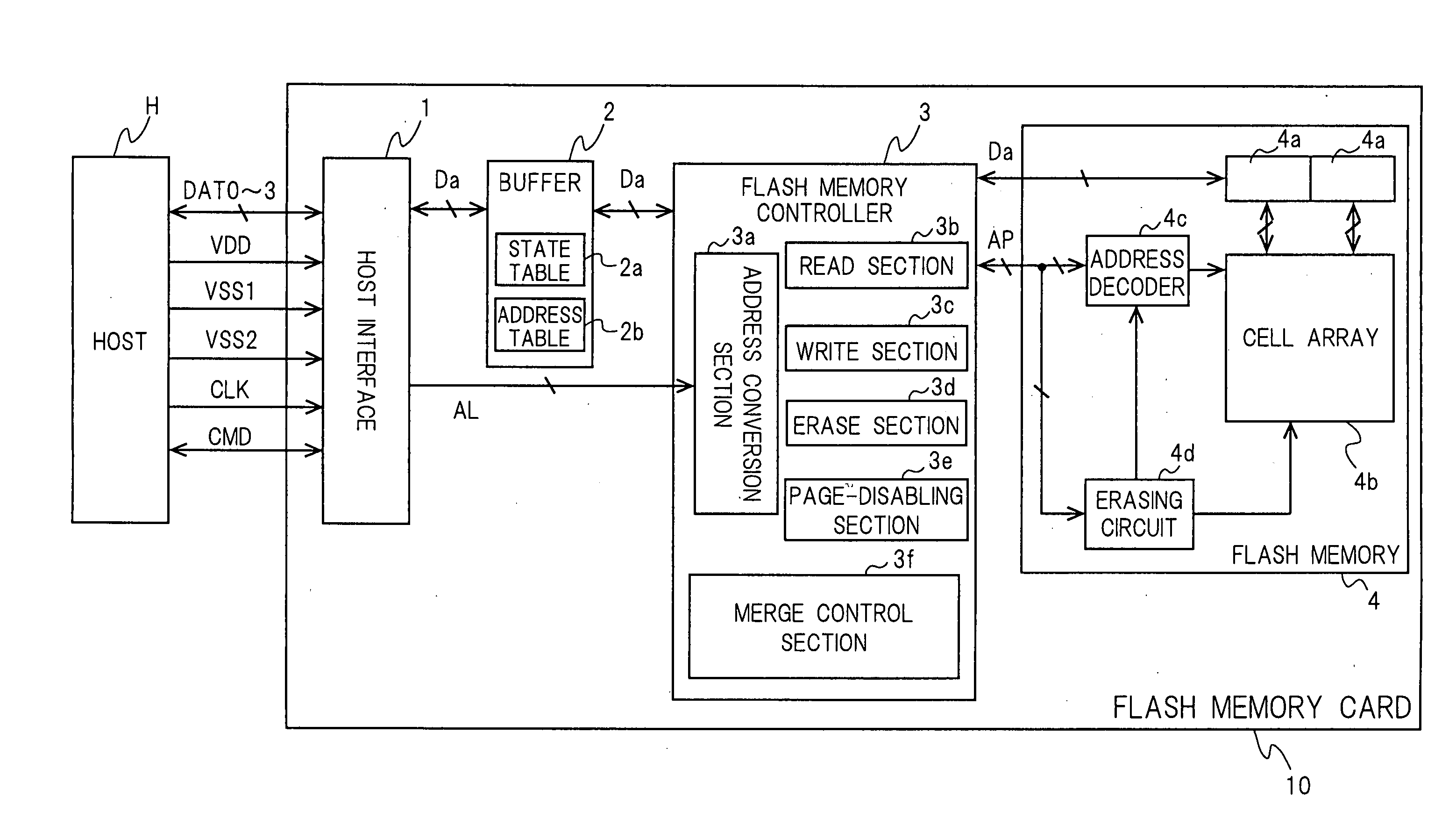
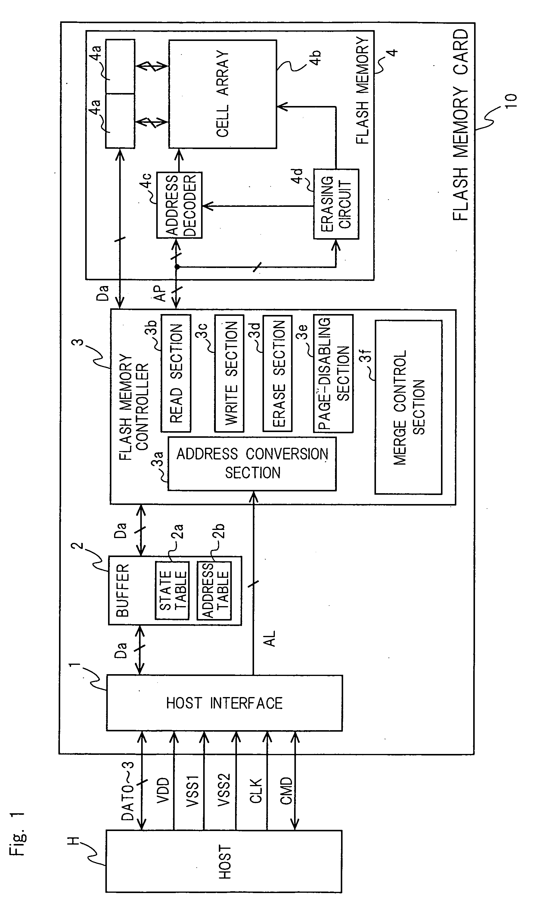
[0092] FIG. 1 is a block diagram showing data exchanges between a flash memory card 10 of the present invention and a host H. The flash memory card 10 is connected with the host H through the following five types of lines. The lines are composed of nine lines in total; four data lines DAT0-3, a clock line CLK, a power line VDD, two ground lines VSS1 and VSS2, and a command line CMD.
[0093] A host interface 1 is the circuit for performing communications directly with the host H through the above-mentioned nine lines. The host interface 1 receives commands from the host H through the command line CMD and decodes the commands. After that, the host interface performs, for example, the following operations in response to the commands. When a command from the host H is a read command, the host interface 1 decodes the command into the logical address AL of the read target and sends the address to a flash memory controller 3. When a command from the host H is a write command, the host inter...
embodiment 2
[0158] FIG. 8 is a block diagram showing data exchanges between a flash memory card 10A according to Embodiment 2 of the present invention and a host H. The flash memory card 10A according to Embodiment 2 comprises two flash memories in contrast to the counterpart 10 of Embodiment 1 (FIG. 1). In FIG. 8, components similar to those of Embodiment 1 are marked with the same reference symbols as those of Embodiment 1. Furthermore, the description of Embodiment 1 is cited regarding those similar components.
[0159] A flash memory controller 3A and two flash memories 4A and 4B according to Embodiment 2 are really similar in internal structure to their respective counterparts 3 and 4 of Embodiment 1, and therefore FIG. 1 is cited regarding them.
[0160] The duration of data transfer between the flash memory controller 3A and the flash memory 4A or 4B inside the page buffers 4a is on the order of several tens of nsec. On the other hand, the duration of writing data from the page buffer 4a into ...
embodiment 3
[0166] FIG. 9 is a block diagram showing data exchanges between a flash memory card 10B according to Embodiment 3 of the present invention and a host H. The flash memory card 10B according to Embodiment 3 comprises two flash memories in a manner similar to the counterpart 10A of Embodiment 2 (FIG. 8). In FIG. 9, components similar to those of Embodiment 1 are marked with the same reference symbols as those of Embodiment 1. Furthermore, the description of Embodiment 1 is cited regarding those similar components.
[0167] The two flash memories 4A and 4B according to Embodiment 3 are really similar in internal structure to their counterpart 4 of Embodiment 1, and therefore FIG. 1 is cited regarding them.
[0168] A flash memory controller 3B according to Embodiment 3 substantially includes two internal structures each of which is similar to that of its counterpart 3 according to Embodiment 1. Of the internal structures similar to that of the flash memory controller 3 according to Embodiment...
PUM
 Abstract
Description
Claims
Application Information