Plasma display panel

a technology of display panel and plasma, which is applied in the direction of gas discharge vessel/container, electrode, gas-filled discharge tube, etc., can solve the problems of limited structural intensity, pdp is liable to be bent or twisted, and the chassis base does not disperse it in a suitable manner

Inactive Publication Date: 2004-10-14
SAMSUNG SDI CO LTD
View PDF3 Cites 38 Cited by
  • Summary
  • Abstract
  • Description
  • Claims
  • Application Information

AI Technical Summary

Problems solved by technology

However, when the display device undergoes impact or vibration of external loading, the PDP is liable to be bent or twisted, and this exhibits a structural weakness thereof.
With the PDP display device, the chassis base endures most of the loads and the distortions pursuant thereto, but is limited in its structural intensity.
When an excessive external load is applied to the display device, the chassis base does not disperse it in a suitable manner.
The excessive external load reaches the PDP, and particularly the barrier ribs mounted within the PDP, so that the substrates or the barrier ribs are broken or ruptured.
The resulting abnormal discharge can break the dielectric, causing device failure.
Consequently, a vibration is induced between front substrate 9 and rear substrate 13 while incurring noises, and this impairs the product quality and the structural stability of the PDP.

Method used


Image

  • Plasma display panel
  • Plasma display panel
  • Plasma display panel

Examples


first embodiment

[0086] As described above, the structural intensity of the PDP according to the present invention is reinforced by the reinforcing barrier ribs so that when an external loading, such as bending, twisting, impact, and vibration, is applied to the PDP, the breakage of the PDP like the collapsing of the barrier ribs can be minimized. Accordingly, even though the external load not absorbed by the chassis base is applied to the PDP, the breakage thereof can be prevented, and the discharge cells can be operated in a stable manner.

second embodiment

[0087] A PDP according to the present invention will be now explained in detail.

[0088] FIGS. 10 and 11 are a partial exploded perspective view of a PDP according to a second embodiment of the present invention and a schematic plan view thereof, respectively.

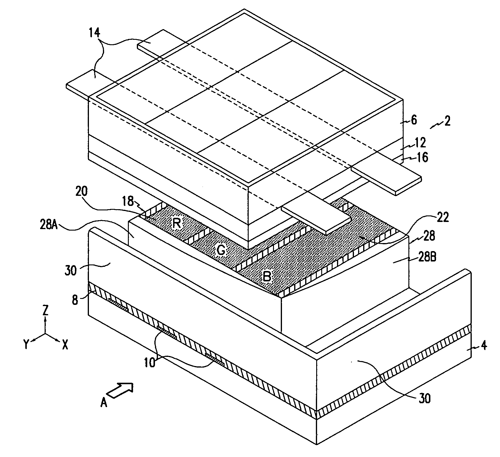
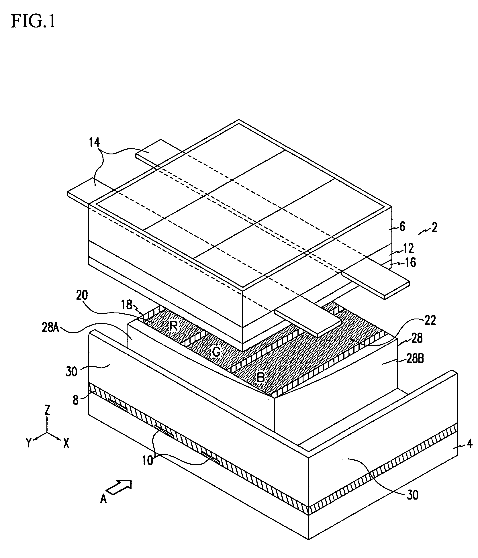
[0089] As shown in the drawings, the PDP includes first and second substrates 52, 54 facing each other with some distance, and discharge cells 56R, 56G, 56B disposed between the substrates 52, 54. Each cell 56 has an independent discharge mechanism to emit visible rays, and display the desired color image.

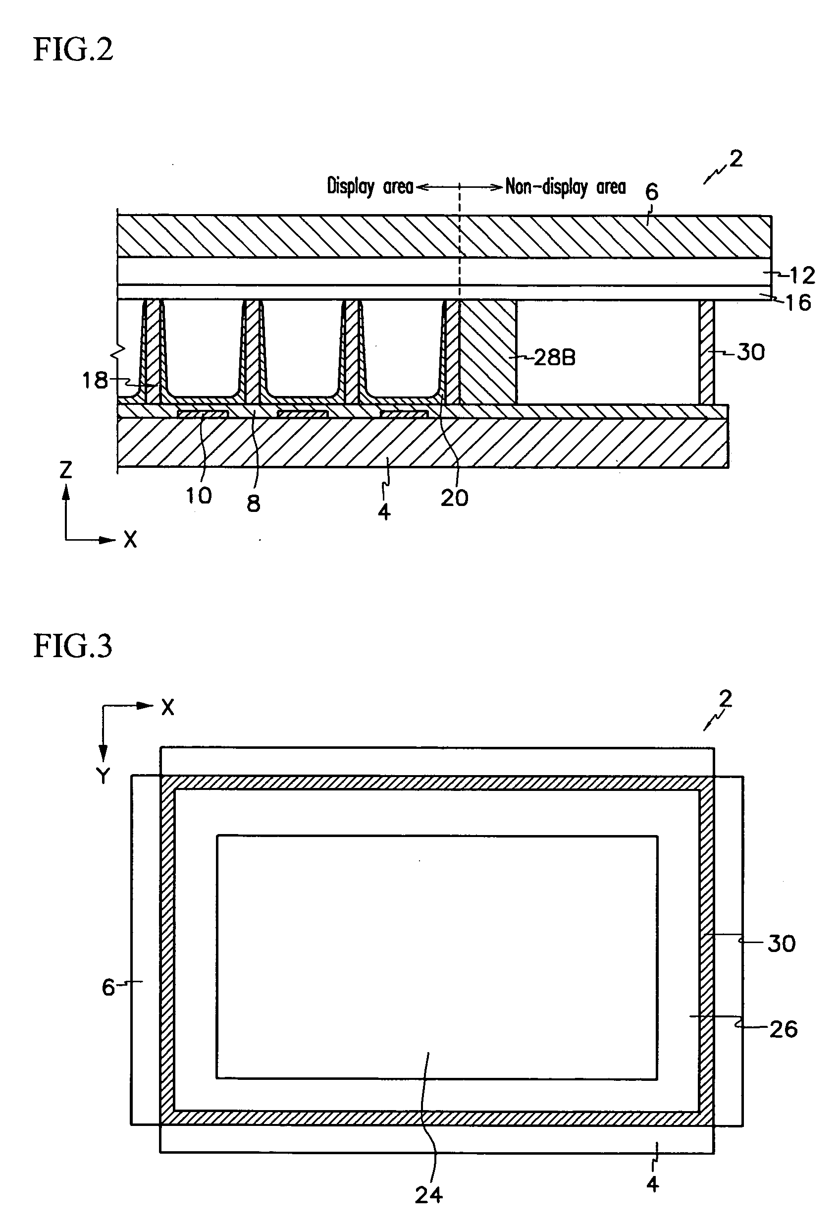
[0090] Specifically, address electrodes 58 are formed on the inner surface of first substrate 52 while proceeding in a direction (in the Y direction of the drawing). Bottom dielectric layer 60 is formed on the entire inner surface of first substrate 52 while covering address electrodes 58. Address electrodes 58 are stripe-patterned, and spaced apart from each other at a predetermined distance while proceeding parallel to each ot...


PUM


Abstract

A plasma display panel includes first and second substrates spaced apart from each other at a distance while proceeding substantially parallel to each other. The first and the second substrates have a display area and a non-display area. A plurality of address electrodes are formed on the first substrate, and covered by a dielectric layer. Main barrier ribs are arranged between the substrates to form discharge cells. Phosphor layer is formed with the discharge cells. A plurality of discharge sustain electrodes are formed on the surface of the second substrate facing the first substrate, and covered by a dielectric layer. Reinforcing barrier ribs are arranged at the non-display area while surrounding the display area, and connected to the main barrier ribs with an outer structure curved toward the outside of the substrates.

Description

[0001] This application claims priority to and the benefit of Korea Patent Applications No.: 2003-0023090 filed on Apr. 11, 2003 and No. 2003-0050276 filed on Jul. 22, 2003, both filed at the Korean Intellectual Property Office, the entire contents of which are incorporated herein by reference.[0002] (a) Field of the Invention[0003] The present invention relates to a plasma display panel (PDP), and in particular, to a barrier rib for a plasma display panel.[0004] (b) Description of Related Art[0005] Recently, the PDP has been spotlighted as a candidate for a wide screen display devices, such as a wall-mounted TVs and others. The PDP performs its displaying operation with a discharge mechanism realized at discharge cells. The discharge cells are formed by barrier ribs placed on the substrates in a suitable pattern (stripe or lattice).[0006] As is well known in the art, the PDP is supported by a chassis base mounting a plurality of driving circuit boards at its rear side, and a front ...

Claims


Application Information

Patent Timeline
Patent Type & Authority Applications(United States)
IPC IPC(8): H01J11/12H01J11/22H01J11/24H01J11/26H01J11/34H01J11/36
CPCH01J11/12H01J11/36H01J2211/368
Inventor WOO, SEOK-GYUNKANG, TAE-KYOUNG
Owner SAMSUNG SDI CO LTD
Why Eureka
Try Eureka