Failure analyzer

a failure analyzer and analyzer technology, applied in the direction of individual semiconductor device testing, semiconductor/solid-state device testing/measurement, instruments, etc., can solve the problems of reducing the resolution of the sample, the method is described, and the difficulty in stably mounting the sample on the stag

Inactive Publication Date: 2004-10-28
RENESAS TECH CORP
View PDF12 Cites 21 Cited by
  • Summary
  • Abstract
  • Description
  • Claims
  • Application Information

AI Technical Summary

Benefits of technology

[0015] Because of inclusion of the analysis plate which includes the protrusion functioning as a solid immersion lens and is separate from the sample, it is possible to move the protrusion relative to a failure site in a device layer where a device is to be formed in the sample. Accordingly, an analysis range can be changed, and failure analysis of an arbitrary portion can be easily carried out. Further, since the protrusion functioning as a solid immersion lens does not protrude from the second main surface of the analysis plate, it is possible to stably mount the sample on a stage with the analysis plate interposed therebetween.
[0017] Since the solid immersion lens is embedded in the stage, it is possible to move the solid immersion lens relative to a device layer where a device is to be formed in the sample. Accordingly, an analysis range can be changed, and failure analysis of an arbitrary portion can be easily carried out. Further, since the surface of the solid immersion lens includes the portion which is flat and is exposed to be flush with the first main surface of the stage, it is possible to stably mount the sample on the stage and the solid immersion lens.

Problems solved by technology

Ever-increasing use of a multilayer structure for interconnection of a semiconductor device such as an LSI causes difficulties in evaluating or analyzing the semiconductor device from a direction of a top surface of a semiconductor substrate, so that evaluation or analysis of the semiconductor device must be carried out from a direction of a back surface of the semiconductor substrate.
Nevertheless, the method of Ippolito reference has a disadvantage that a resolution is occasionally reduced considerably due to possible creation of a clearance between the semiconductor substrate and the SIL.
In this regard, the method described in Ippolito reference has a further disadvantage of having difficulties in stably mounting the sample on the stage because of inclusion of the substantially hemispherical SIL on the back surface of the semiconductor substrate which protrudes from the back surface of the semiconductor substrate.
Nevertheless, the protrusion functioning as an SIL in JP2002-18900, which is formed by performing some processes on the semiconductor substrate itself, cannot be moved.

Method used


Image

  • Failure analyzer
  • Failure analyzer
  • Failure analyzer

Examples


Embodiment Construction

[0032] First Preferred Embodiment

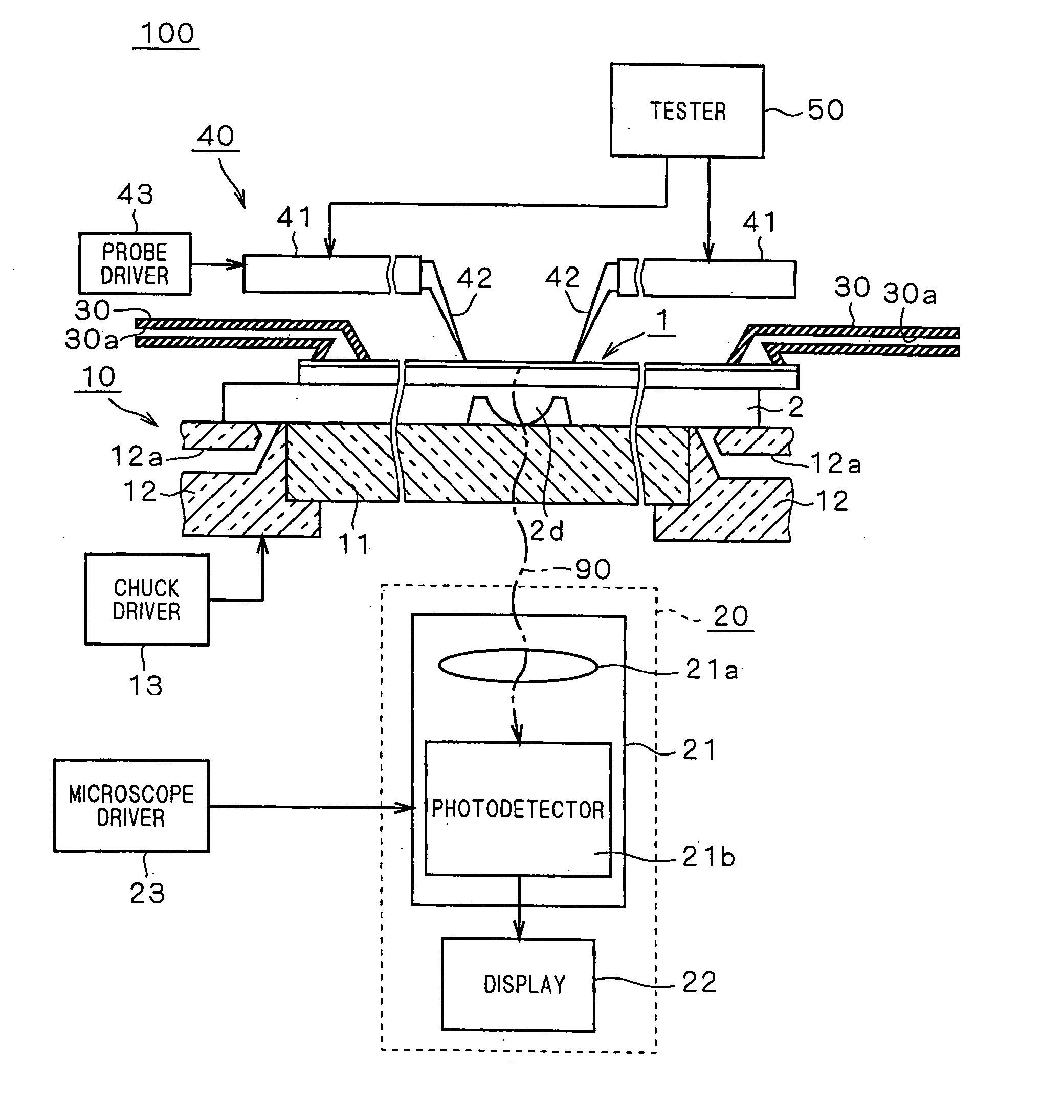
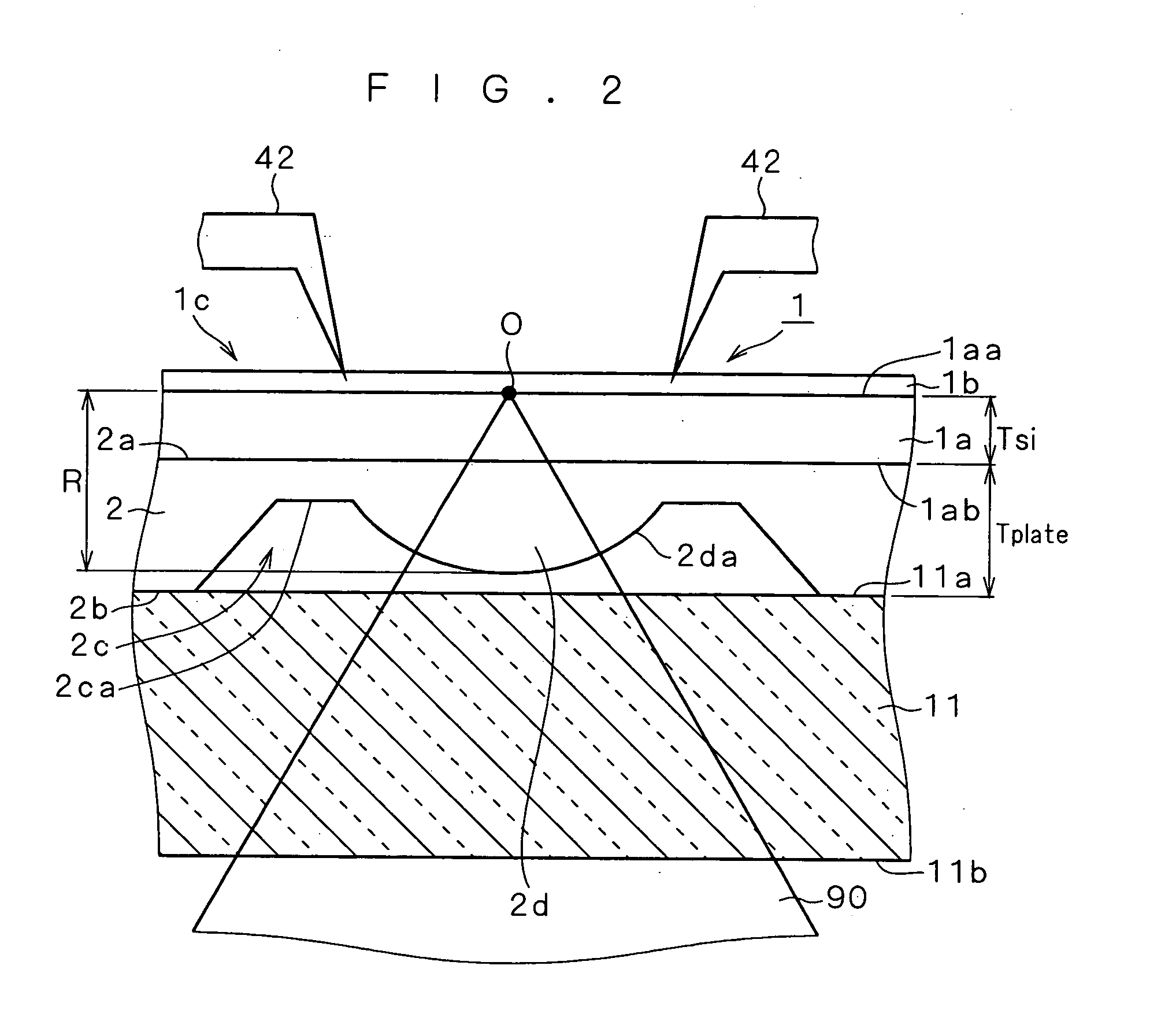
[0033] FIG. 1 illustrates a structure of a failure analyzer 100 according to a first preferred embodiment of the present invention. FIG. 2 is a magnified view of a portion of the structure illustrated in FIG. 1. As illustrated in FIGS. 1 and 2, the failure analyzer 100 according to the first preferred embodiment is capable of carrying out emission analysis on a sample 1. The failure analyzer 100 according to the first preferred embodiment includes an analysis plate 2 including an SIL, an SIL driver 10, a failure detector 20, a microscope driver 23, a sample support member 30, a prober 40 and a tester 50. It is noted that out of the elements illustrated in FIGS. 1 and 2, the sample 1, the analysis plate 2, the sample support member 30, a stage 11, a chuck 12 and a probe card 41 are illustrated in section. Additionally, details of the stage 11, the chuck 12 and the probe card 41 will be later provided.

[0034] FIG. 3 is a plan view of a structure of the ...


PUM


Abstract

A sample (1) is mounted on a stage (11) with an analysis plate (2) interposed therebetween. A recess (2c) is provided in a main surface (2b) of the analysis plate (2), and a protrusion (2d) functioning as a solid immersion lens is provided on a bottom surface (2ca) of the recess (2c). The protrusion (2d) does not protrude from the main surface (2b) of the analysis plate (2). Because of provision of the analysis plate (2) which includes a solid immersion lens and is separate from the sample (1), an analysis range can be changed. Further, since the protrusion (2d) does not protrude from the main surface (2b) of the analysis plate (2), the sample (1) can be stably mounted on the stage (11) with the analysis plate (2) interposed therebetween.

Description

[0001] 1. Field of the Invention[0002] The present invention relates to a failure analyzer utilizing a solid immersion lens.[0003] 2. Description of the Background Art[0004] Ever-increasing use of a multilayer structure for interconnection of a semiconductor device such as an LSI causes difficulties in evaluating or analyzing the semiconductor device from a direction of a top surface of a semiconductor substrate, so that evaluation or analysis of the semiconductor device must be carried out from a direction of a back surface of the semiconductor substrate. Typical techniques for analyzing a failure from a direction of a back surface include: emission analysis in which a failures is analyzed by detecting a feeble light emitted from a spot of current leakage; an OBIC (optical beam induced current) analysis or OBIRCH (optical beam induced resistance change) analysis in which a failure site is specified by converting a current or change in power supply current which is induced by irradi...

Claims


Application Information

Patent Timeline
Patent Type & Authority Applications(United States)
IPC IPC(8): G01R31/302G01R31/28G01R31/311H01L21/66
CPCG01R31/311H01L22/00
Inventor KOYAMA, TOHRUKOMORI, JUNKO
Owner RENESAS TECH CORP
Why Eureka
Try Eureka