Semiconductor laser cladding layers

Inactive Publication Date: 2004-11-11
MAXION TECH
View PDF6 Cites 11 Cited by
  • Summary
  • Abstract
  • Description
  • Claims
  • Application Information

AI Technical Summary

Problems solved by technology

Conventional semiconductor laser designs suffer from unwanted heat buildup in the active region.
Although conventional cladding layers may

Method used


Image

  • Semiconductor laser cladding layers
  • Semiconductor laser cladding layers
  • Semiconductor laser cladding layers

Examples


example 2

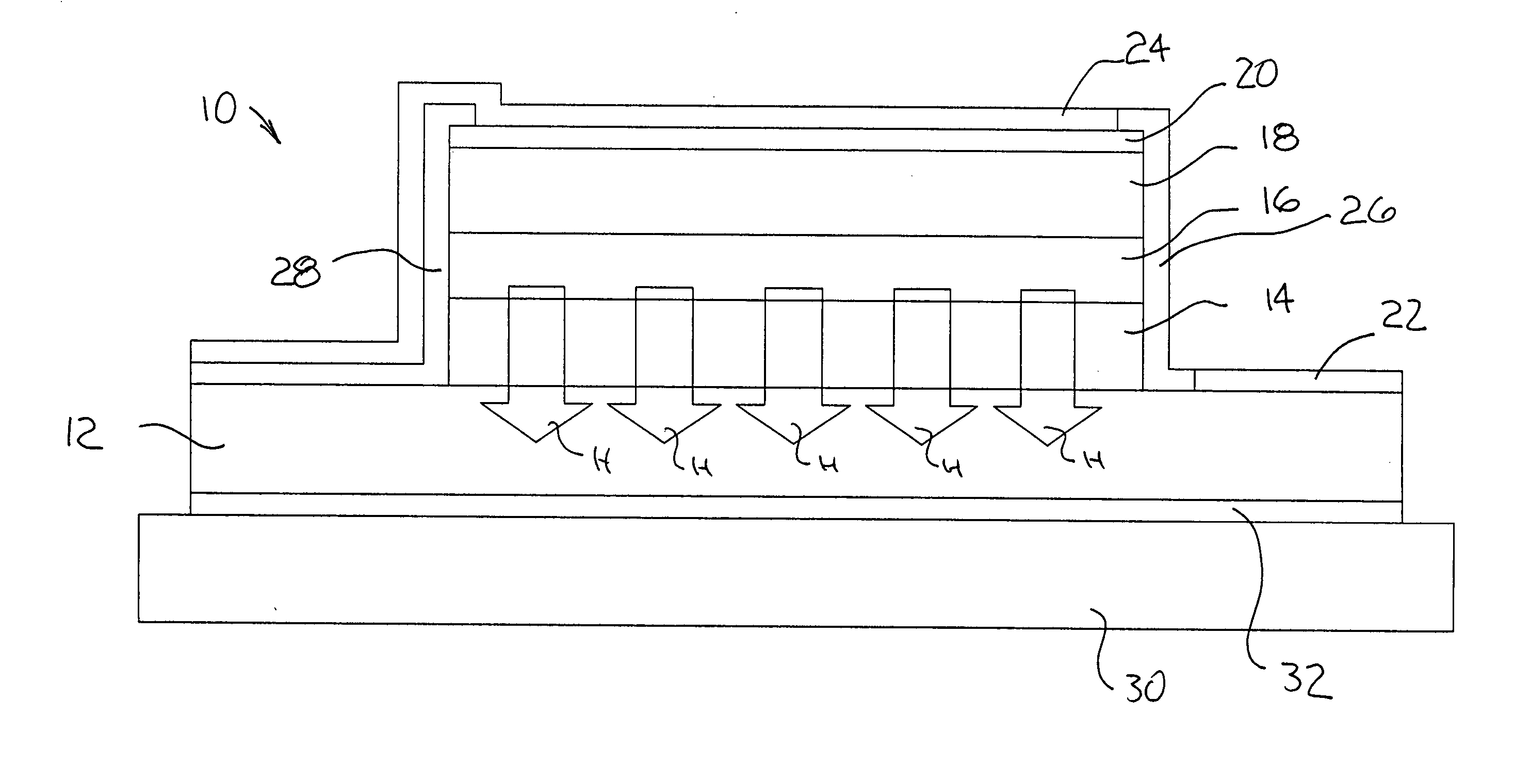
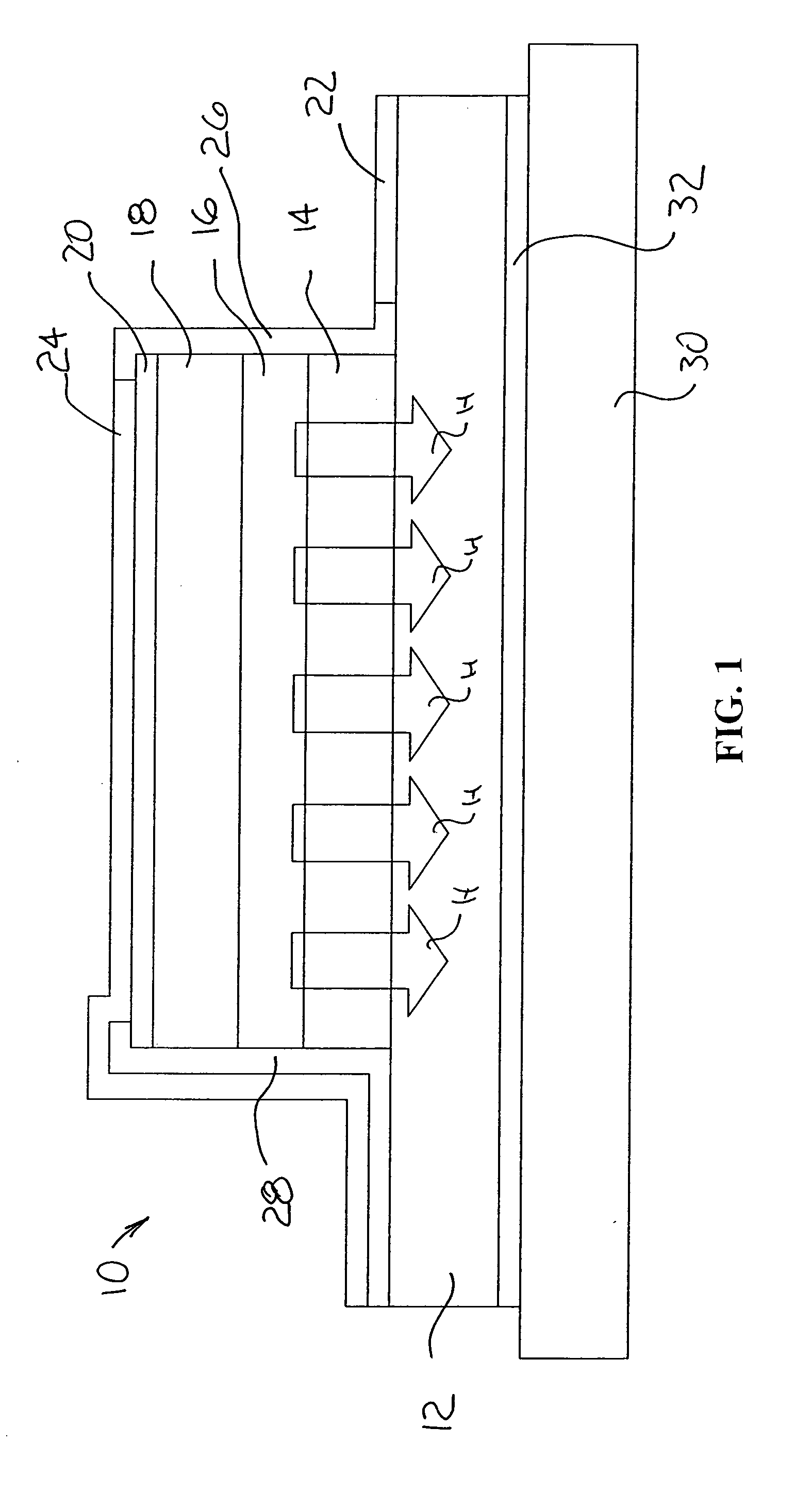
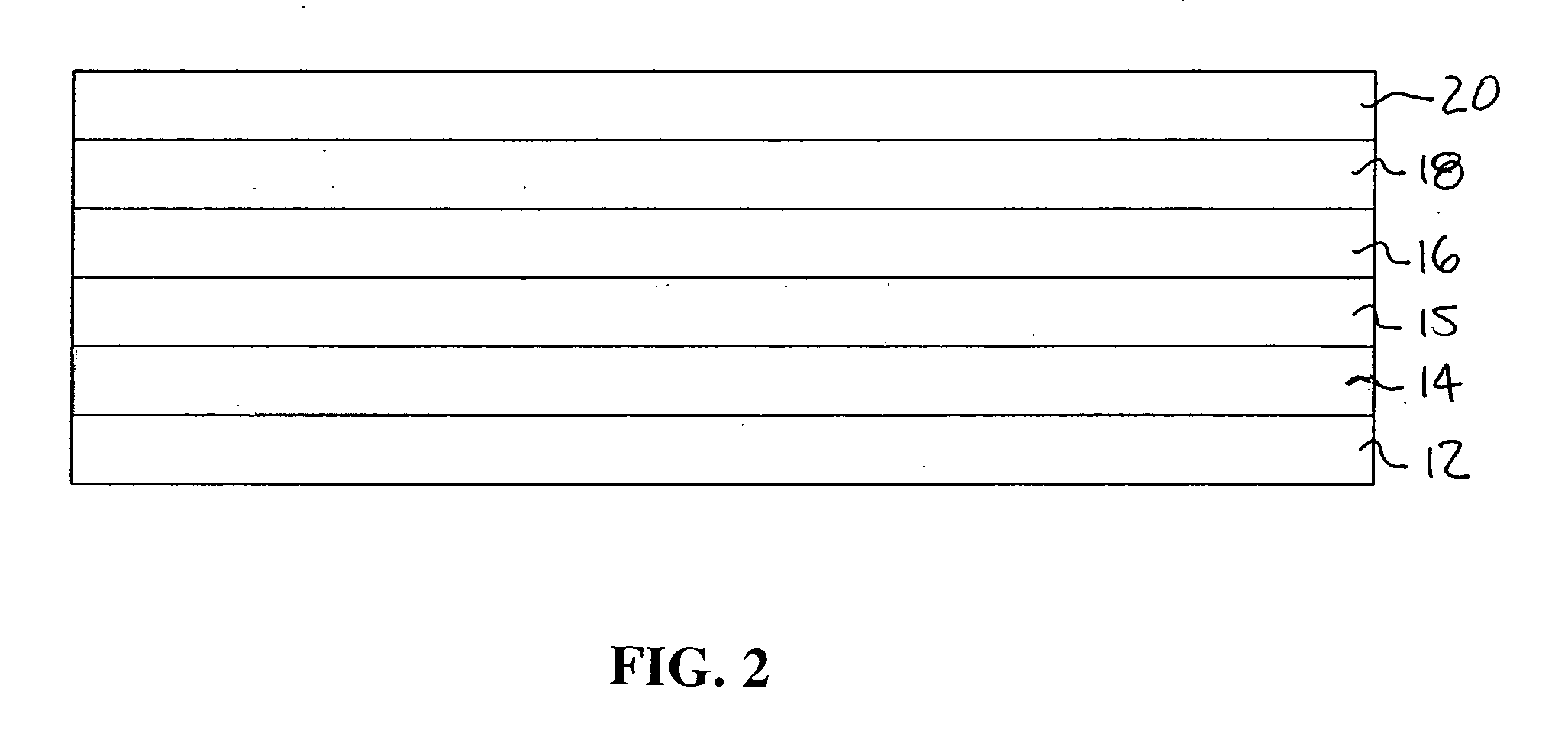
[0057] An operational test of the AlSb / AlAs SL cladding was conducted. An interband cascade laser was fabricated in which the top cladding layer was composed of a 503 period (30 .ANG. AlSb) / (2.73 .ANG. AlAs) SL doped with Be. The intent of this design is to mount laser diodes top-side down on a copper heat sink. Hence the use of the low thermal resistance cladding material for the top cladding layer. X-ray diffraction measurements on this wafer show good crystal quality for the AlSb / AlAs SL cladding layer, as well as the rest of the epitaxial structure.

example 3

[0058] Another operational test of the AlSb / AlAs SL cladding was conducted. An interband cascade laser was fabricated in which the bottom cladding layer was composed of an undoped 613 period (30 .ANG. AlSb) / (2.73 .ANG. AlAs) SL. X-ray diffraction measurements made on this sample also show good crystal quality for the AlSb / AlAs SL cladding as well as the rest of the laser structure growth on top. Measurements made on top-side up mounted lasers show about a 40% reduction in thermal resistance between the active region and heat sink, as compared to devices using AlSb / InAs SL top and bottom cladding layers.

example 4

[0059] A further operational test was conducted in a similar manner as Example 3, except for changes in the P-doped GaSb bottom contact layer that have negligible effect on the thermal properties of the laser device. The crystal quality and thermal resistance characteristics are similar to those of the sample of Example 3.


PUM


Abstract

Cladding layers for semiconductor lasers provide improved heat transfer and optical confinement properties. The cladding layers may comprise superlattices such as AlSb/GaAs, AlSb/AlAs, AlSb/GaSb/AlAs, AlGaSb/AlGaAs and AlSb/AlGaAs. The cladding layers may also comprise Al-As-Sb ternary alloys or Al-Ga-As-Sb quaternary alloys. Such cladding layers may be used in interband cascade lasers or other types of semiconductor lasers to significantly increase heat flow out of the active light-emitting region of the device, while providing improved optical confinement characteristics.

Description

[0001] This application claims the benefit of U.S. Provisional Patent Application Ser. No. 60 / 468,833 filed May 8, 2003, which is incorporated herein by reference.[0002] The present invention relates to semiconductor laser cladding layers, and more particularly relates to cladding layer materials for use in devices such as interband cascade (IC) lasers to provide improved heat transfer and optical confinement characteristics.BACKGROUND INFORMATION[0003] Semiconductor lasers have cladding layers which serve to provide optical confinement for the active region of the laser, and which may also serve as electrical current conductors for the device. For example, in edge-emitting interband cascade lasers, cladding layers are provided on either side of the active region. Such cladding layers may comprise doped AlSb / InAs superlattices having thicknesses of about 2 .mu.m. These cladding layers transport charge between the electrical contacts and the active region. They also provide refractiv...

Claims


Application Information

Patent Timeline
IPC IPC(8): H01S5/00H01S5/024H01S5/32H01S5/34
CPCB82Y20/00H01S5/02272H01S5/024H01S5/3216H01S5/3401H01S5/0237
Inventor BRUNO, JOHN D.TOWNER, FREDERICK JAY
Owner MAXION TECH
Why Eureka
Try Eureka