Direct-patterned optical waveguides on amorphous silicon films

a technology of amorphous silicon film and optical waveguide, applied in the direction of optical waveguide light guide, instruments, optics, etc., can solve the problem of relatively large losses and achieve the effect of reducing the refractive index of the selected region

Inactive Publication Date: 2004-12-02
LAWRENCE LIVERMORE NAT SECURITY LLC
View PDF9 Cites 27 Cited by
  • Summary
  • Abstract
  • Description
  • Claims
  • Application Information

AI Technical Summary

Problems solved by technology

A fundamental problem with p-Si waveguides, however, is that they characteristically exhibit relatively large losses due to a variety of effects, including grain boundary induced optical scatter.
Apart from the cost and complexity of the process, this approach is problematic in that H diffusion in a-Si is strongly temperature dependent, with modest temperature increases .about.100 Celsius producing sufficient interdiffusion,to eliminate the H concentration gradients over modest periods of time.

Method used


Image

  • Direct-patterned optical waveguides on amorphous silicon films
  • Direct-patterned optical waveguides on amorphous silicon films
  • Direct-patterned optical waveguides on amorphous silicon films

Examples


Embodiment Construction

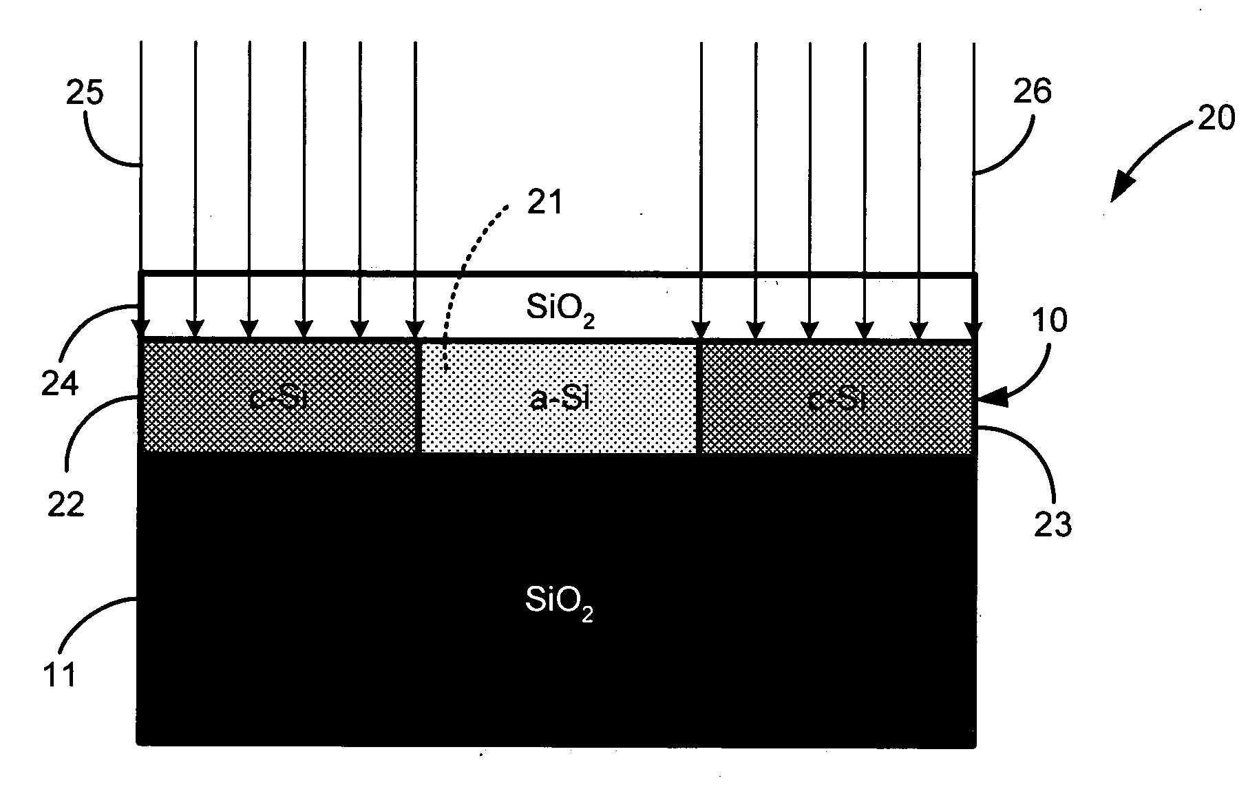
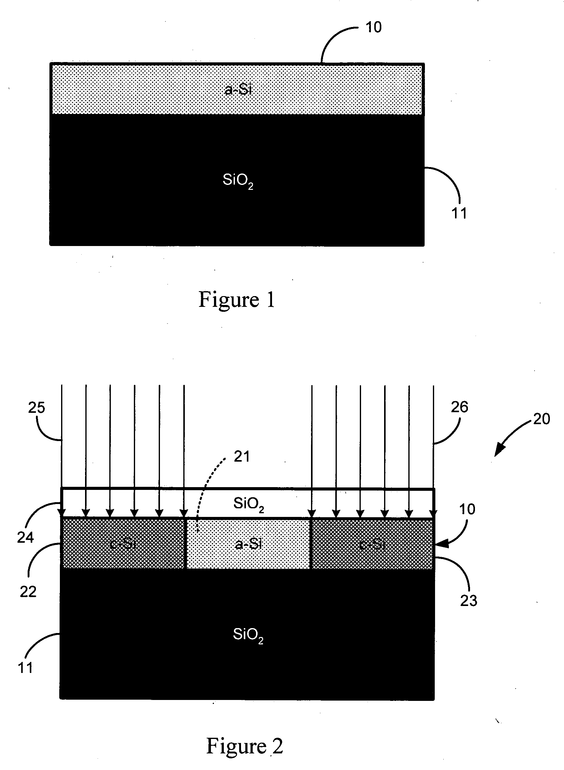
[0020] The present invention is generally directed to an optical waveguide architecture and fabrication method thereof, having an amorphous silicon (a-Si) core region bounded by polycrystalline silicon (p-Si) cladding regions for operation over the spectral range spanning the communication wavelength bands in the range from about 1.2 to about 1.6 microns. In this spectral region, the optical refractive index of a-Si is up to about 20% greater than p-Si, with the amorphous phase having the larger index, n.sub.a.apprxeq.4, and the crystalline phase the lower refractive index n.sub.c.apprxeq.3.2. Such an index differential enables waveguide operation, i.e. optical signal propagation through the higher refractive index a-Si core as bounded by the lower refractive index p-Si cladding.

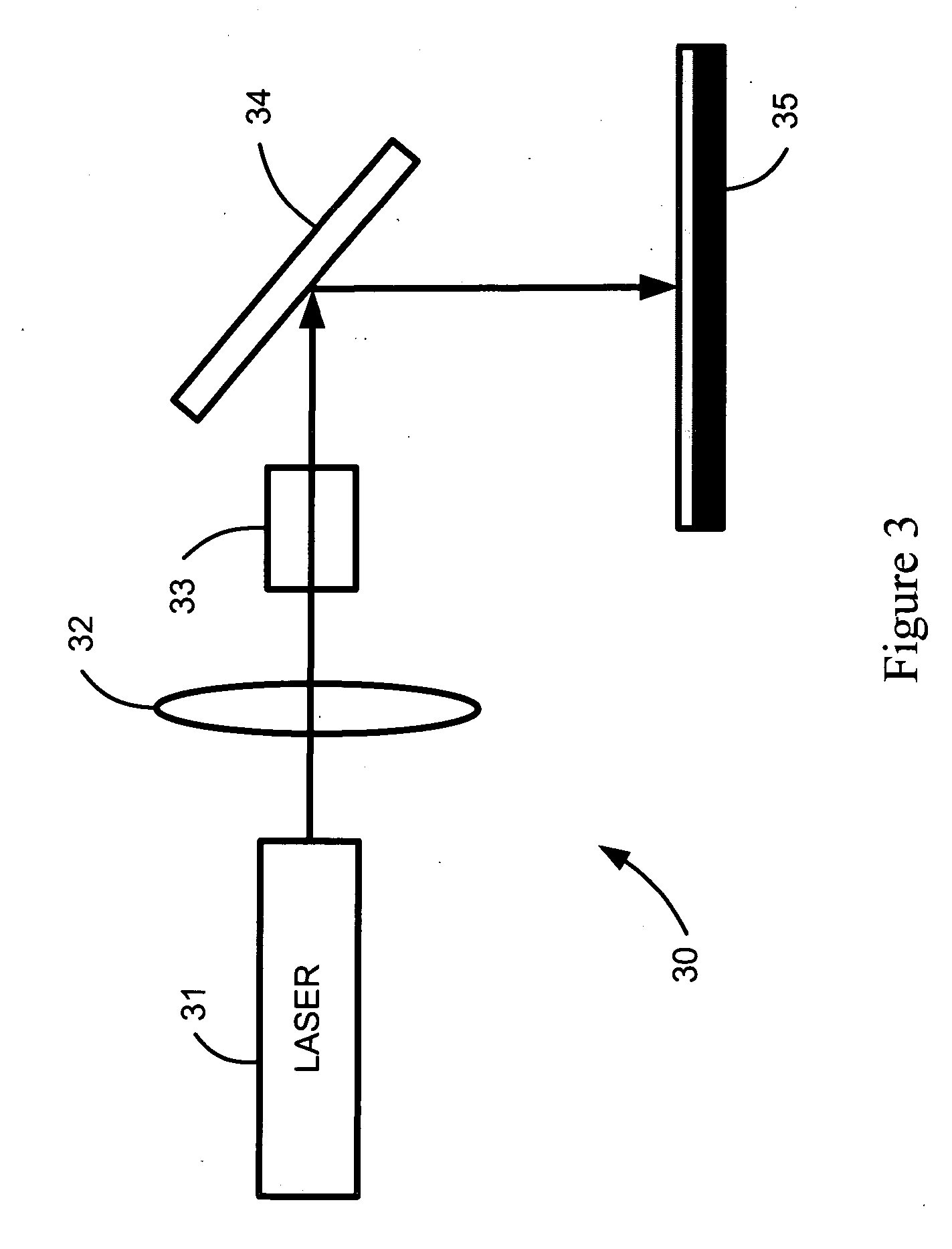
[0021] FIG. 2, shows an exemplary embodiment of the waveguide architecture of the present invention, generally indicated at 20, and having an intermediate silicon (Si) layer 10 formed (such as by thin film d...


PUM


Abstract

An optical waveguide structure is formed by embedding a core material within a medium of lower refractive index, i.e. the cladding. The optical index of refraction of amorphous silicon (a-Si) and polycrystalline silicon (p-Si), in the wavelength range between about 1.2 and about 1.6 micrometers, differ by up to about 20%, with the amorphous phase having the larger index. Spatially selective laser crystallization of amorphous silicon provides a mechanism for controlling the spatial variation of the refractive index and for surrounding the amorphous regions with crystalline material. In cases where an amorphous silicon film is interposed between layers of low refractive index, for example, a structure comprised of a SiO2 substrate, a Si film and an SiO2 film, the formation of guided wave structures is particularly simple.

Description

I. CLAIM OF PRIORITY IN PROVISIONAL APPLICATION[0002] This application claims priority in provisional application filed on May 30, 2003 entitled "Efficient direct writing technique for the patterning of optical waveguides and photonic integrated circuits: novel application of low temperature laser processing to the formation of guided wave structures in amorphous silicon thin films" Ser. No. 60 / 475213, by Stephen P. Vernon et al.II. FIELD OF THE INVENTION[0003] The present invention relates to optical waveguides and fabrication methods thereof, and more particularly to an optical waveguide architecture and a fabrication method in which an amorphous silicon core region and polycrystalline silicon cladding regions are formed from an amorphous silicon layer, with the cladding formed by direct patterned crystallization of selected areas of the a-Si layer.III. BACKGROUND OF THE INVENTION[0004] The use of amorphous silicon (a-Si) for optical device applications is rapidly expanding as the...

Claims


Application Information

Patent Timeline
Patent Type & Authority Applications(United States)
IPC IPC(8): G02B6/12G02B6/132
CPCG02B6/132G02B2006/12061G02B2006/12169G02B2006/12173
Inventor VERNON, STEVEBOND, TIZIANA C.BOND, STEVEN W.POCHA, MICHAEL D.HAU-RIEGE, STEFAN
Owner LAWRENCE LIVERMORE NAT SECURITY LLC
Why Eureka
Try Eureka