

Semiconductor device and manufacturing method thereof
- Summary
- Abstract
- Description
- Claims
- Application Information
AI Technical Summary
Benefits of technology
Problems solved by technology
Method used
Image

Examples
first embodiment
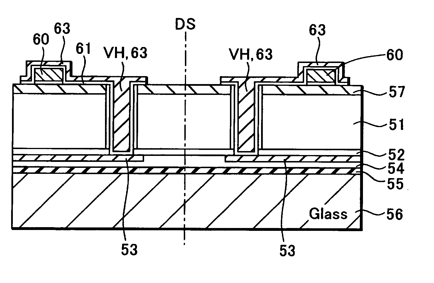
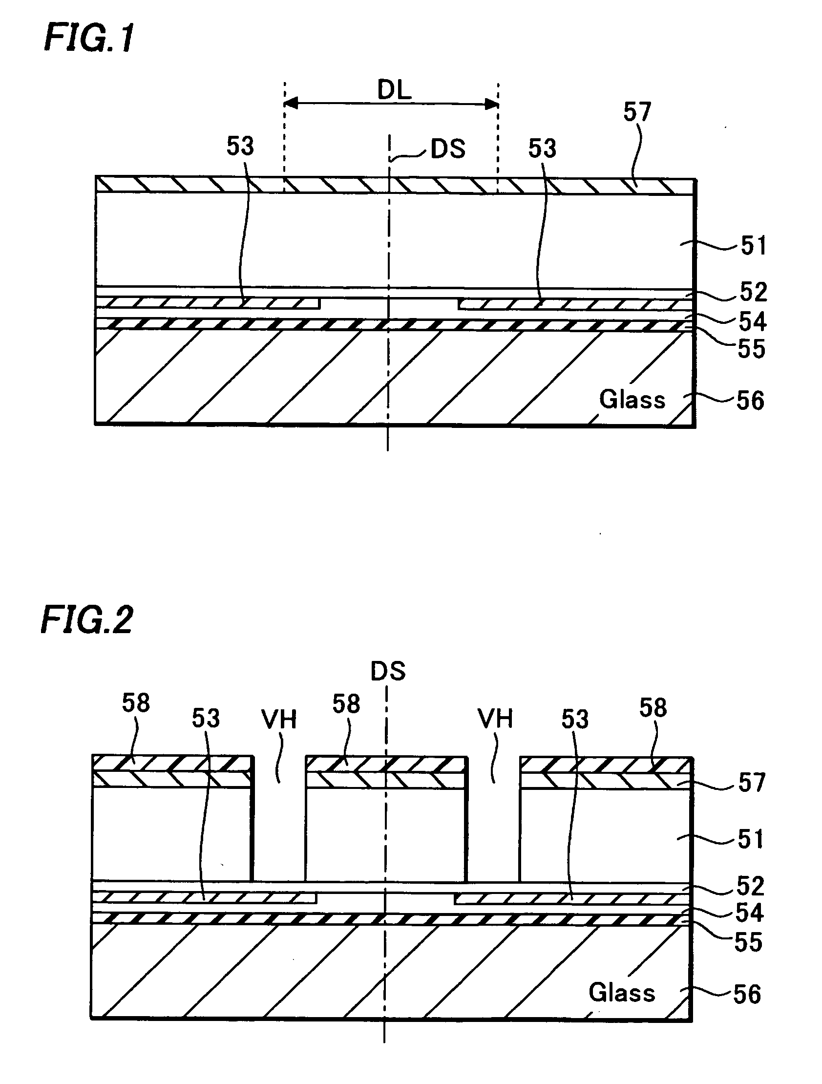
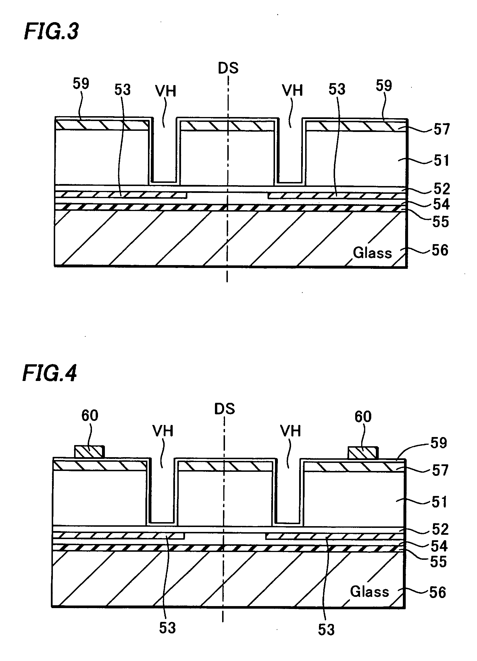
[0046] Next, this invention will be described in detail, referring to figures hereinafter. First, a structure of the semiconductor device will be described. FIG. 12 is a cross-sectional view of the semiconductor device separated into individual dice by dicing a silicon wafer along a dicing line after process steps to be described hereinafter. DS in FIG. 12 denotes a center of the dicing line.
[0047] A silicon die 51A is a CCD (Charge Coupled Device) image sensor chip, for example. A pad electrode 53 is formed on a surface which is a first surface of the silicon die 51A through an interlayer insulation film 52 such as a BPSG (Boro-Phospho Silicate Glass) film. The pad electrode 53 is formed by extending a normal pad electrode used for wire bonding to the dicing line region and is also called an extended pad electrode.
[0048] The pad electrode 53 is covered with a passivation film 54 made of a silicon nitride film, for example. A glass substrate 56 is bonded through a resin layer 55 ma...
second embodiment
[0086] Next, this invention will be described in detail, referring to figures hereinafter. First, a structure of the semiconductor device will be described. FIG. 15 is a cross-sectional view of the semiconductor device separated into individual dice by dicing a silicon wafer along a dicing line after process steps to be described below.
[0087] DS in FIG. 15 denotes a center of the dicing line. The same reference numerals are used in FIG. 15 as in FIG. 12 for the common components, and detailed explanations on them are omitted.
[0088] Cushioning pads 60A are formed over the entire back surface of the silicon die 51A except for regions adjacent to the via holes VH in this embodiment. The wiring 63 extends from the via hole VH onto the cushioning pad 60A and terminate on the cushioning pad 60A. As a result, coverage of the wiring 64 and the solder mask 65 formed on the cushioning pad 60A is improved compared with the first embodiment. The other structural features are the same as in the...
PUM
 Abstract
Description
Claims
Application Information