Semiconductor injection locked lasers and method

a technology of injection locking laser and semiconductor, which is applied in the field of lasers, can solve the problems of limiting the application of injection locking laser systems to the laboratory environment, and limiting the performance of fiber-optic systems

Inactive Publication Date: 2005-01-20
ARCHCOM TECH
View PDF7 Cites 31 Cited by
  • Summary
  • Abstract
  • Description
  • Claims
  • Application Information

AI Technical Summary

Benefits of technology

[0016] In one embodiment of this aspect, at least one laser section is a DFB laser. In another embodiment, at least one laser section is a DBR laser. In another embodiment, the first laser is adapted for injection locking the second laser section and the second laser section is modulated with electrical input signal for emitting light modulated in response to the input signal. In another embodiment, the electrical contact of the injection locked second laser is divided into two or more laser sections.
[0017] In various embodiments of the aspects of the invention, the operating wavelength of the two sections is current tuned to achieve optical injection locking; when locked the modulation bandwidth is increased from about 5 GHz to about 23 GHz.

Problems solved by technology

In some of these applications, the nonlinearity and low modulation bandwidth of the semiconductor lasers limit the performance of the fiber-optic systems.
However, injection locking laser systems have generally been restricted to the laboratory environment.
This restriction exists because experiments involving injection locking typically require two separately packaged lasers.
However, light losses and optical coupling efficiency can impact the maximum injection ratio.
Configuring and mounting these various system components on an optical bench further limits the portability of injection locked lasers.
Although suitable for research applications, large-scale multi-component laser systems are not suitable for many applications outside the laboratory.
In particular, the size constraints and the need for multiple optically linked system elements render these configurations impractical for many telecommunications applications.

Method used


Image

  • Semiconductor injection locked lasers and method
  • Semiconductor injection locked lasers and method
  • Semiconductor injection locked lasers and method

Examples


Embodiment Construction

[0032] The presently preferred and alternative embodiments of the invention, including the best mode for practicing the invention known at this time, are now described in detail in connection with the accompanying drawings. It is, however, expressly noted that the present invention is not limited to these embodiments, but rather the intention is that modifications that are apparent to the person skilled in the art and equivalents thereof are also included.

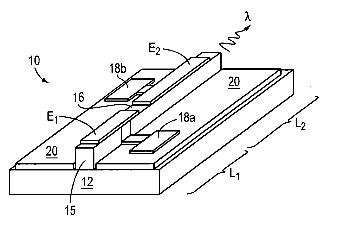
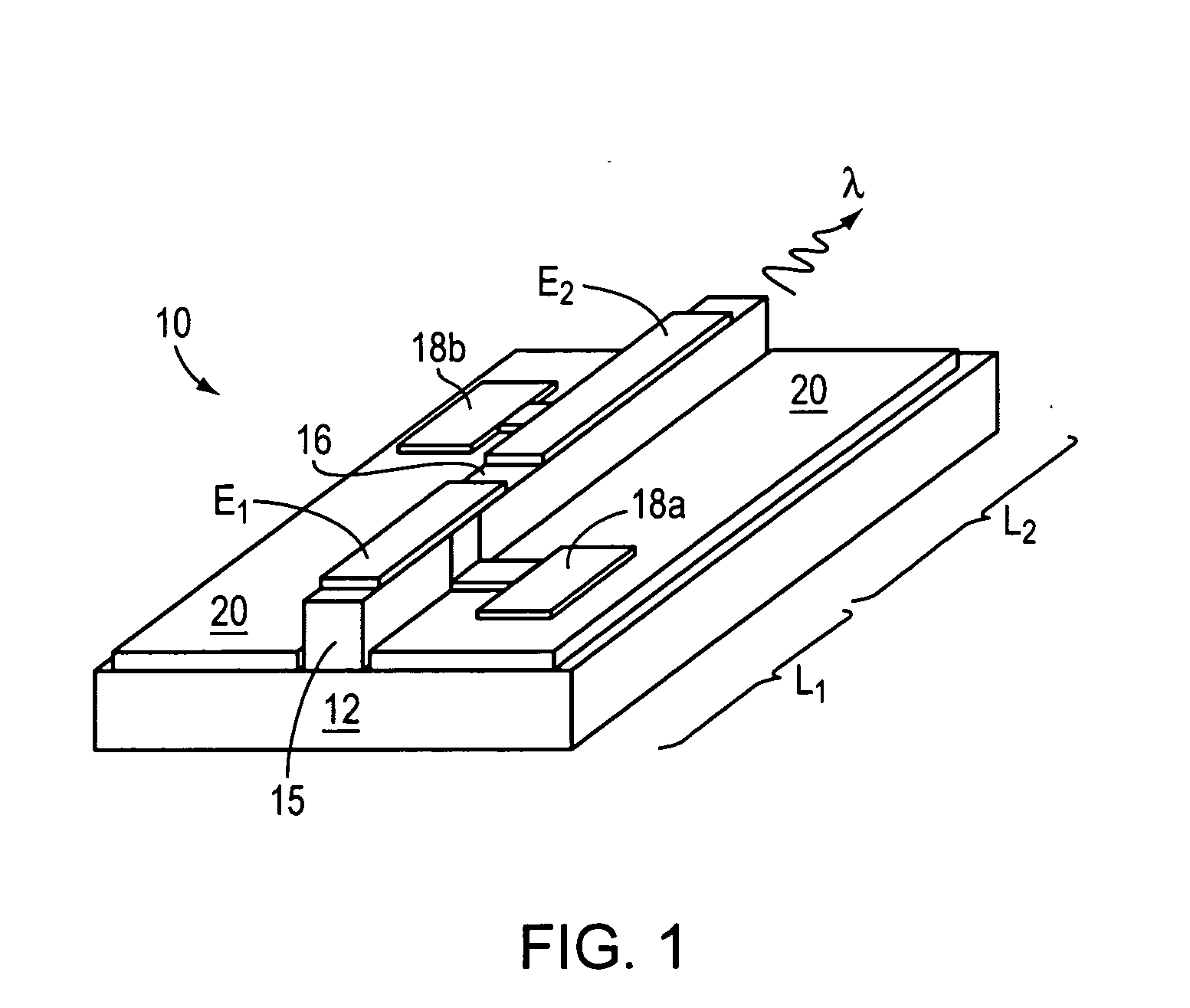
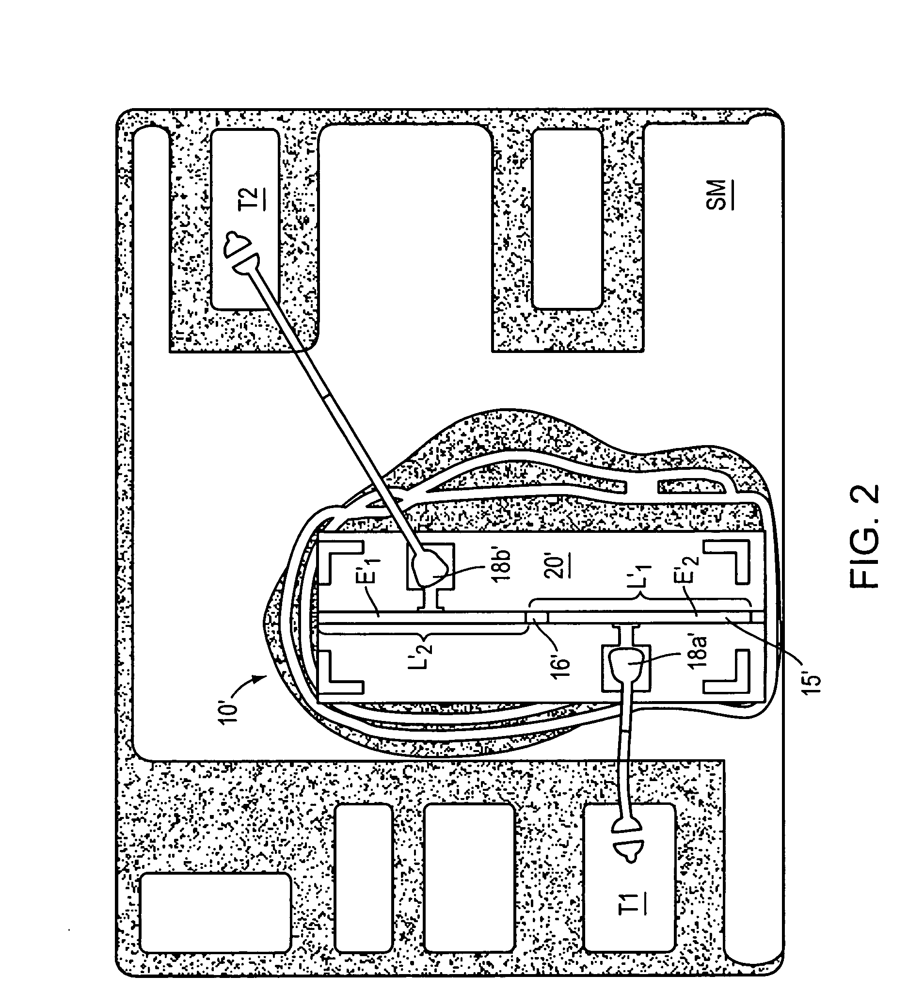
[0033] In part, aspects of the invention are designed to improve semiconductor laser bandwidth, noise reduction, and linearity without significantly increasing manufacturing cost. Such results may be achieved through monolithic injection locked laser embodiments that incorporate coupled lasers in tandem. Specifically, a single unitary structure has been developed that enables the benefits of injection locking without using two, physically separate lasers as part of a larger optical system. Thus, in part, the invention relates to a...


PUM


Abstract

In one aspect, the invention relates to a semiconductor laser. The laser includes a substrate and an elongate unitary laser structure disposed on the substrate. In turn, the elongate unitary laser structure includes a first laser section, a second laser section, and a plurality of shared layers. The first and second laser sections are capable of lasing independently of each other. The shared layers form both the first laser section and the second laser section. The first laser section is adapted for injection locking the second laser section.

Description

CROSS-REFERENCE TO RELATED APPLICATIONS [0001] This application claims the benefits of provisional U.S. patent application Ser. No. 60 / 474,570 filed on May 30, 2003, the disclosure of which is hereby incorporated herein by reference in its entirety.GOVERNMENT SUPPORT [0002] This invention was made with Government support under Grant No. DAAD17-01-C-0077, awarded by the DARPA RFLICS Program. The Government has certain rights in this invention.FIELD OF THE INVENTION [0003] The invention relates generally to the field of lasers. Specifically, the invention relates to semiconductor lasers and injection locking techniques. BACKGROUND OF THE INVENTION [0004] The development of optical fiber based communication systems has led to numerous advances over conventional wire based technology. In particular, increases in available bandwidth have made new services and applications possible. Some of these increases in bandwidth derive from the ability to multiplex multiple channels of information....

Claims


Application Information

Patent Timeline
Patent Type & Authority Applications(United States)
IPC IPC(8): H01S3/14H01S5/00H01S5/026H01S5/40
CPCH01S5/4006H01S5/026
Inventor JUNG, THOMASLIOU, KANG-YIHSUNG, HYUK-KEETISHININ, DENISTSANG, WON T.WU, MING C.
Owner ARCHCOM TECH
Why Eureka
Try Eureka