Terahertz wave modulating device with light control flat panel silicon photonic crystal and method thereof

A silicon photonics, flat-panel technology, applied in the field of terahertz wave applications, to meet the needs of communication, compact structure, and large modulation bandwidth

Inactive Publication Date: 2009-09-30
CHINA JILIANG UNIV
View PDF0 Cites 7 Cited by
  • Summary
  • Abstract
  • Description
  • Claims
  • Application Information

AI Technical Summary

Problems solved by technology

At present, the application of BWO is either used for spectrum analysis or imaging detection, but there is no such technology at home and abroad to apply BWO to THz wave communication

Method used


Image

  • Terahertz wave modulating device with light control flat panel silicon photonic crystal and method thereof
  • Terahertz wave modulating device with light control flat panel silicon photonic crystal and method thereof
  • Terahertz wave modulating device with light control flat panel silicon photonic crystal and method thereof

Examples


Embodiment 1

[0022] Terahertz wave modulation at 0.62THz frequency:

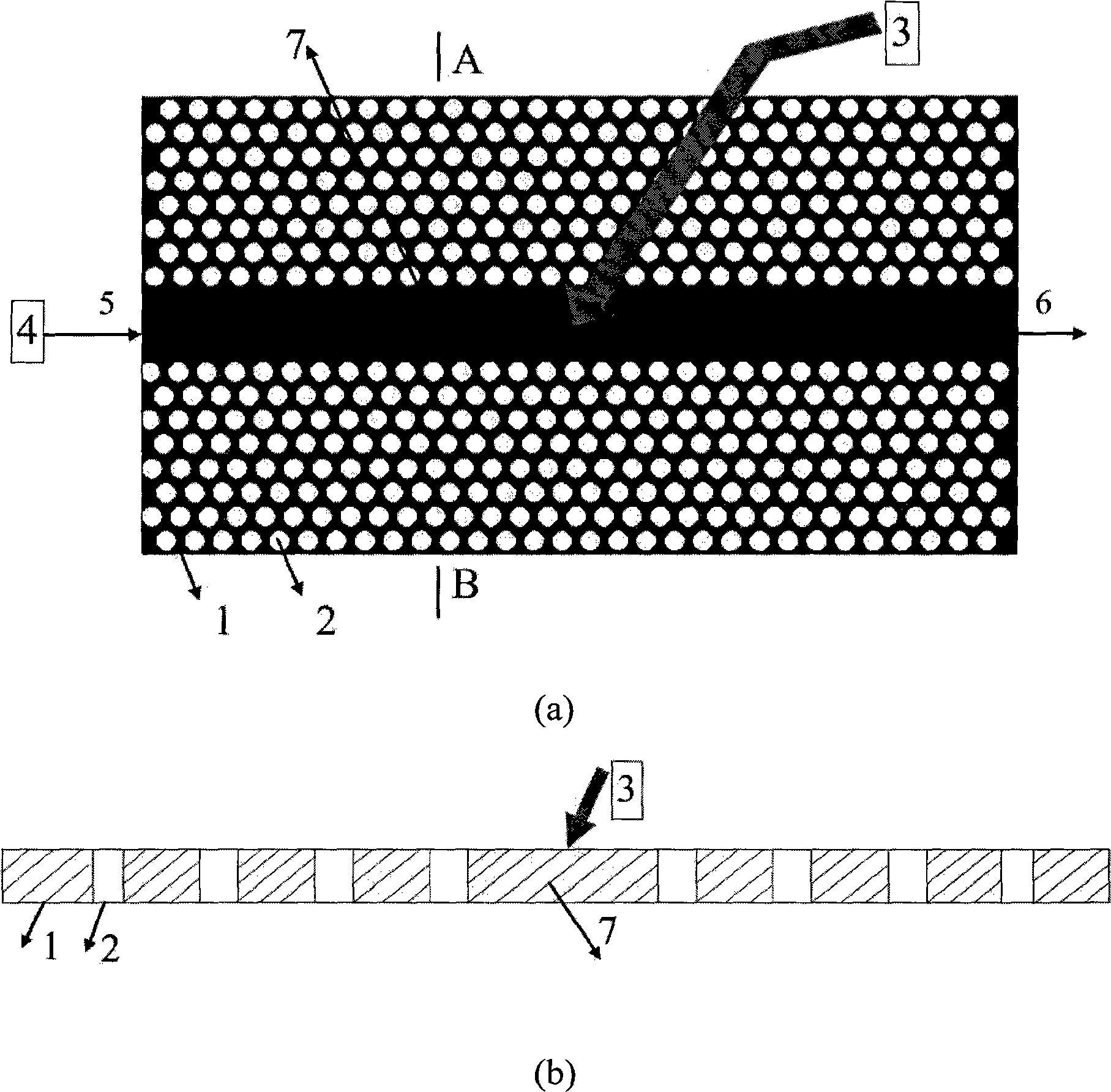
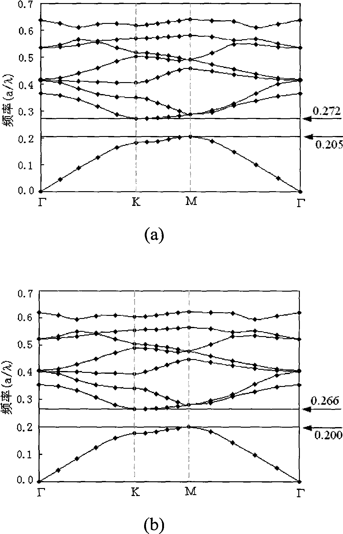
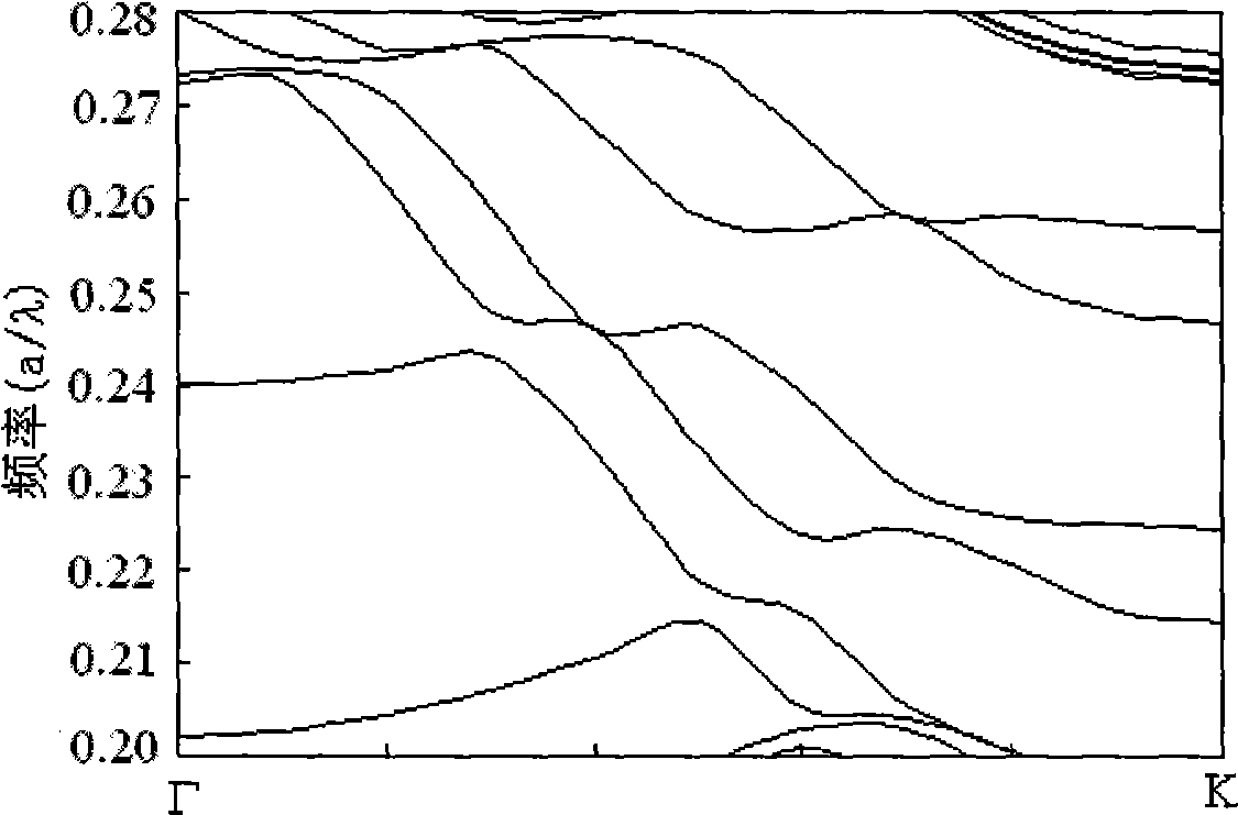
[0023] The return wave oscillator BWO sold by Microtech is selected, and the return wave tube model is selected as QS1-900ov81 (the frequency is tunable in the 0.60-0.90THz frequency band), and the computer controls the BWO output wave to change within the 0.60-0.90THz frequency band. The designed silicon photonic crystal period is 100μm, the refractive index of silicon photonic crystal is 3.5, the thickness of silicon wafer is 0.5mm, the resistivity of silicon is 10000Ωcm, the radius of photonic crystal hole is 30μm, and the width of the line defect area of ​​flat silicon photonic crystal is 3 air holes For the cycle, the frequency of the terahertz wave used for terahertz communication is selected as 0.62THz, the operating wavelength of the semiconductor laser is 808nm, and the power is 10mW. The steady-state transmission of terahertz waves in slab silicon photonic crystals is shown in the attached Figure 4 (a); when ...


PUM

PropertyMeasurementUnit
thicknessaaaaaaaaaa
thicknessaaaaaaaaaa
refractive indexaaaaaaaaaa

Abstract

The invention discloses a terahertz wave modulating device with light control flat panel silicon photonic crystal and a method thereof. The terahertz wave modulating device comprises a silicon chip, air holes, a modulated semiconductor laser, a terahertz wave source, an input end of a linear defect area, an output end of the linear defect area, and the linear defect area; the middle of the silicon chip is provided with the linear defect area; the silicon chip on two sides of the linear defect area is provided with the air holes; the silicon chip, the air holes and the linear defect area form the flat panel silicon photonic crystal; the modulated semiconductor laser is arranged above the linear defect area; and terahertz waves emitted by the terahertz wave source are input from the input end of the linear defect area, pass through the linear defect area, and are output from the output end of the linear defect area. The edge of a forbidden band of the flat panel silicon photonic crystal modulates the terahertz waves to realize load signals onto the terahertz waves. The terahertz wave modulating device has the advantages of low transmission loss, large modulation bandwidth, quick modulation speed, high extinction ratio, small size, compact structure, and convenient integration, and meets the communication requirement of the terahertz waves.

Description

technical field [0001] The invention relates to the technical field of terahertz wave applications, in particular to an optically controlled flat-panel silicon photonic crystal terahertz wave modulation device and a method thereof. Background technique [0002] Terahertz (THz, 1THz=10E+12Hz) radiation usually refers to electromagnetic radiation waves with a frequency range from 0.1THz to 10THz. This band is located at the junction of electronics and optics. It occupies a very special position in the electromagnetic spectrum. , has a series of special properties and important academic and application value. Terahertz communication has rich frequency band resources, large bandwidth, good confidentiality, and is not affected by distant electronic interference. It is difficult for a third party to receive terahertz communication signals locally. It can realize confidential communication within the range of 2 to 5Km, transmission The rate can reach 1-10Gb / s and other advantages,...

Claims


Application Information

Patent Timeline
Patent Type & Authority Applications(China)
IPC IPC(8): G02F1/00H04B10/155H04B10/516
Inventor 李九生
Owner CHINA JILIANG UNIV
Why Eureka
Try Eureka