Edge normal process

a normal process and edge technology, applied in the field of inspection systems, can solve the problems of limited defect classification, low yield, and limited benefits of detecting particles

Active Publication Date: 2005-01-20
ONTO INNOVATION INC
View PDF31 Cites 50 Cited by
  • Summary
  • Abstract
  • Description
  • Claims
  • Application Information

AI Technical Summary

Problems solved by technology

It has recently been discovered that edge inspection is important for detecting delamination of thin films, chipping and cracking of the wafer, resist removal metrology, and particle detection that all cause yield issues in a modern fab.
This solution provides limited benefits in detecting particles and chip-outs, and is limited in classifying defects.

Method used


Image

  • Edge normal process
  • Edge normal process
  • Edge normal process

Examples


Embodiment Construction

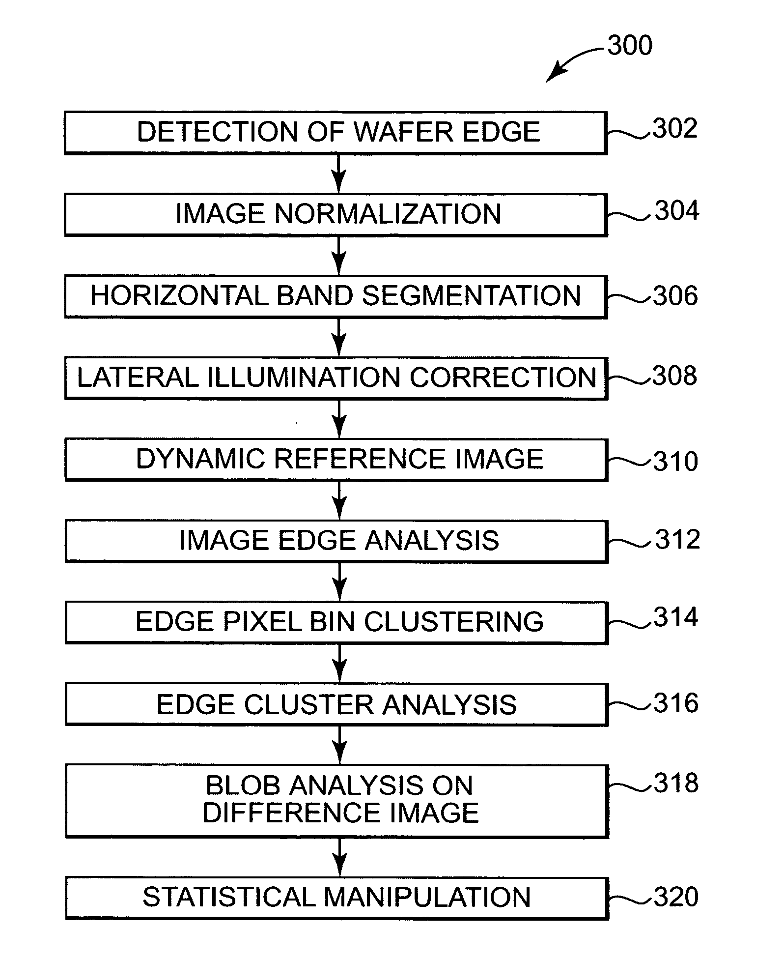
[0025] The edge normal inspection method of the present invention may be used on any of a number of edge inspection systems. The present invention is a method of detecting defects along the wafer edge normal surface. In general, the method of finding defects on the wafer edge normal of the present invention involves the following steps: (1) detection of the wafer edge, (2) image normalization, (3) horizontal band segmentation, (4) lateral illumination correction, (5) creation of a dynamic reference image, (6) image edge analysis, (7) edge pixels bin clustering, (8) edge cluster analysis, (9) blob analysis on difference image, and (10) statistical manipulation.

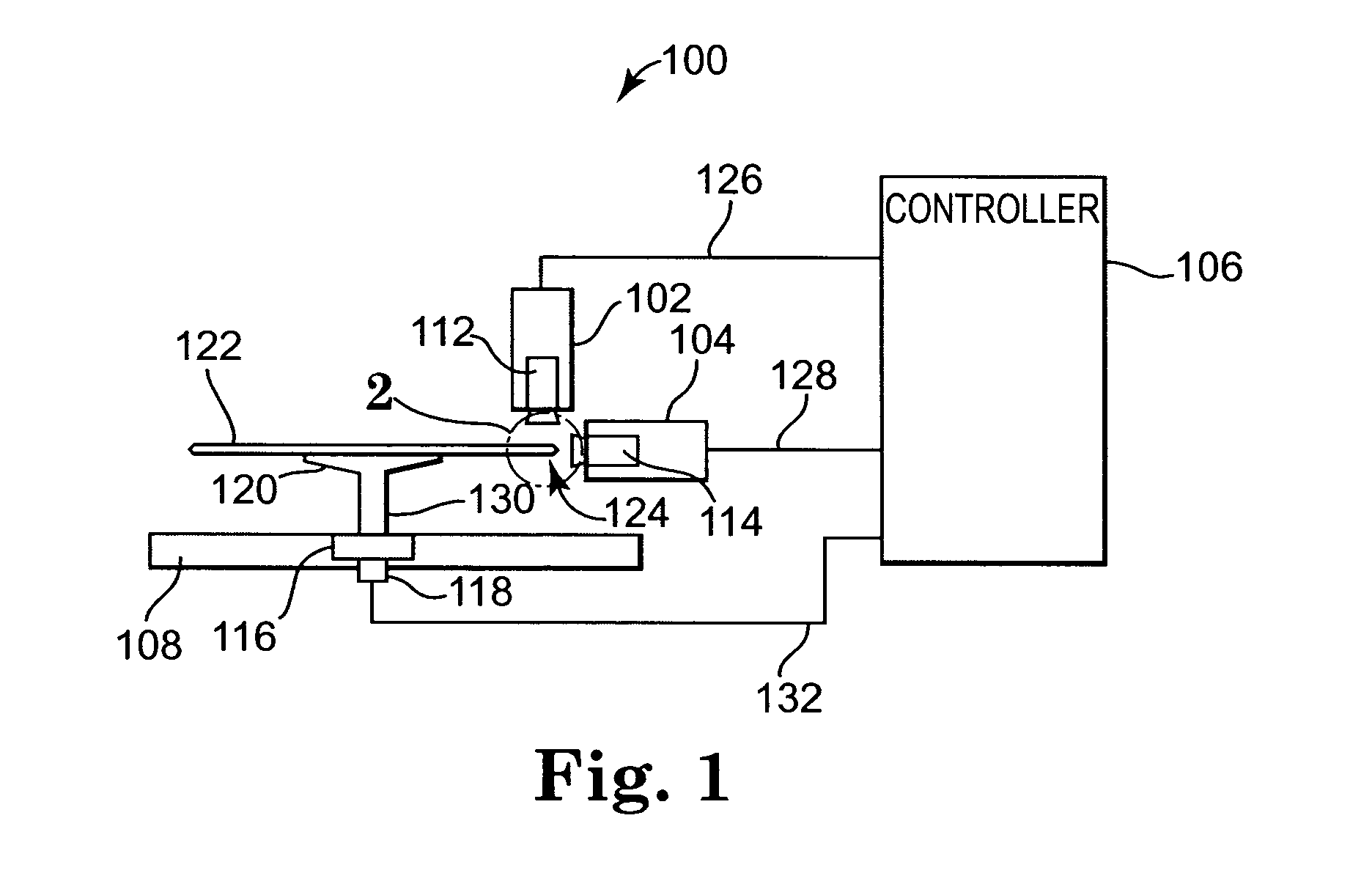
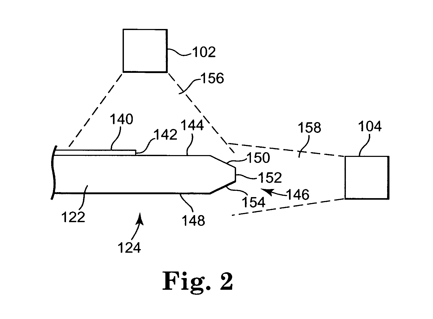
[0026]FIG. 1 is a schematic diagram illustrating one embodiment of an edge inspection system 100. Edge inspection system 100 includes an edge top sensor 102, an edge normal sensor 104, a controller 106, a base 108, and a stage 110. Top edge sensor 102 includes a camera 112, and normal edge sensor 104 includes a camera 114. Sta...


PUM

PropertyMeasurementUnit
field of viewaaaaaaaaaa
depth-of-fieldaaaaaaaaaa
thresholdaaaaaaaaaa

Abstract

An edge inspection method for detecting defects on a wafer edge normal surface includes acquiring a set of digital images which captures a circumference of the wafer. An edge of the wafer about the circumference is determined. Each digital image is segmented into a plurality of horizontal bands. Adjacent edge clusters about the circumference of the wafer are combined into edge pixel bins. The edge pixel bins are analyzed via edge clusters analysis to identify defects. The edge pixel bins are also analyzed via blob analysis to determine defects.

Description

CROSS-REFERENCE TO RELATED APPLICATIONS [0001] This application claims the benefit priority under 35 U.S.C. §119(e) to U.S. Provisional Application Ser. No. 60 / 486,952, filed Jul. 14, 2003 and entitled “EDGE NORMAL PROCESS”.BACKGROUND [0002] 1. Technical Field [0003] The present invention relates to an inspection system that inspects the edge normal surface of a semiconductor wafer or like substrate such as a microelectronics substrate to identify defects therealong. [0004] 2. Background Information [0005] Over the past several decades, the semiconductor has exponentially grown in use and popularity. The semiconductor has in effect revolutionized society by introducing computers, electronic advances, and generally revolutionizing many previously difficult, expensive and / or time consuming mechanical processes into simplistic and quick electronic processes. This boom in semiconductors has been fueled by an insatiable desire by business and individuals for computers and electronics. Th...

Claims


Application Information

Patent Timeline
Patent Type & Authority Applications(United States)
IPC IPC(8): G01N21/95G01R31/26G01R31/28G06K9/00G06T7/00
CPCG01N21/9503G06T2207/30148G06T7/0004G01R31/2831
Inventor SIM, HAK CHUAH
Owner ONTO INNOVATION INC
Why Eureka
Try Eureka