

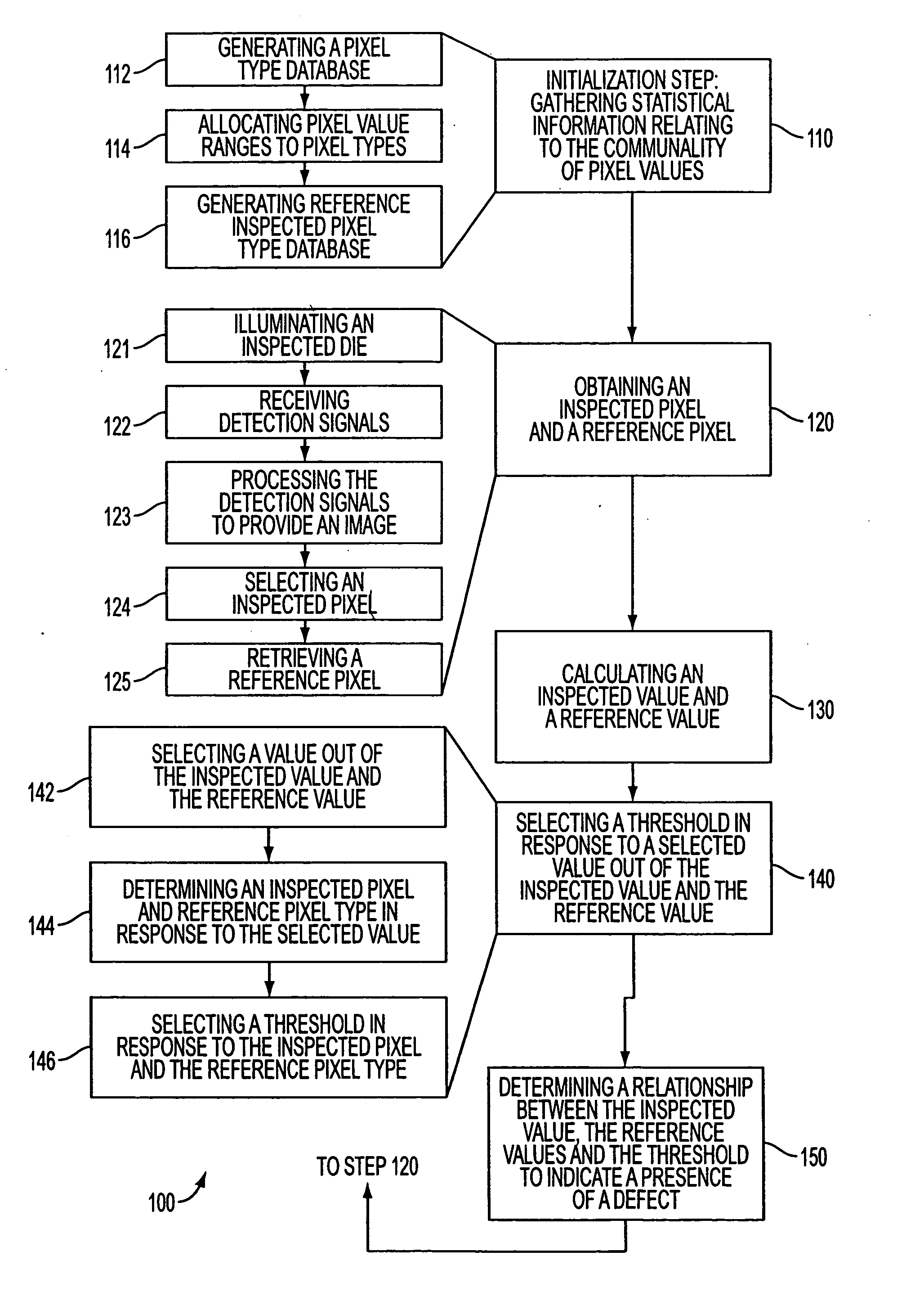
Method for detecting defects
a technology of defect detection and detection method, applied in the field of detection of defects, can solve the problems of erroneous detection of defects, unable to dynamically adjust or tailor the type according to the end-user requirement, and erroneous determination, so as to overcome noise, less erroneous, and less noise
- Summary
- Abstract
- Description
- Claims
- Application Information
AI Technical Summary
Benefits of technology
Problems solved by technology
Method used
Image

Examples
Embodiment Construction
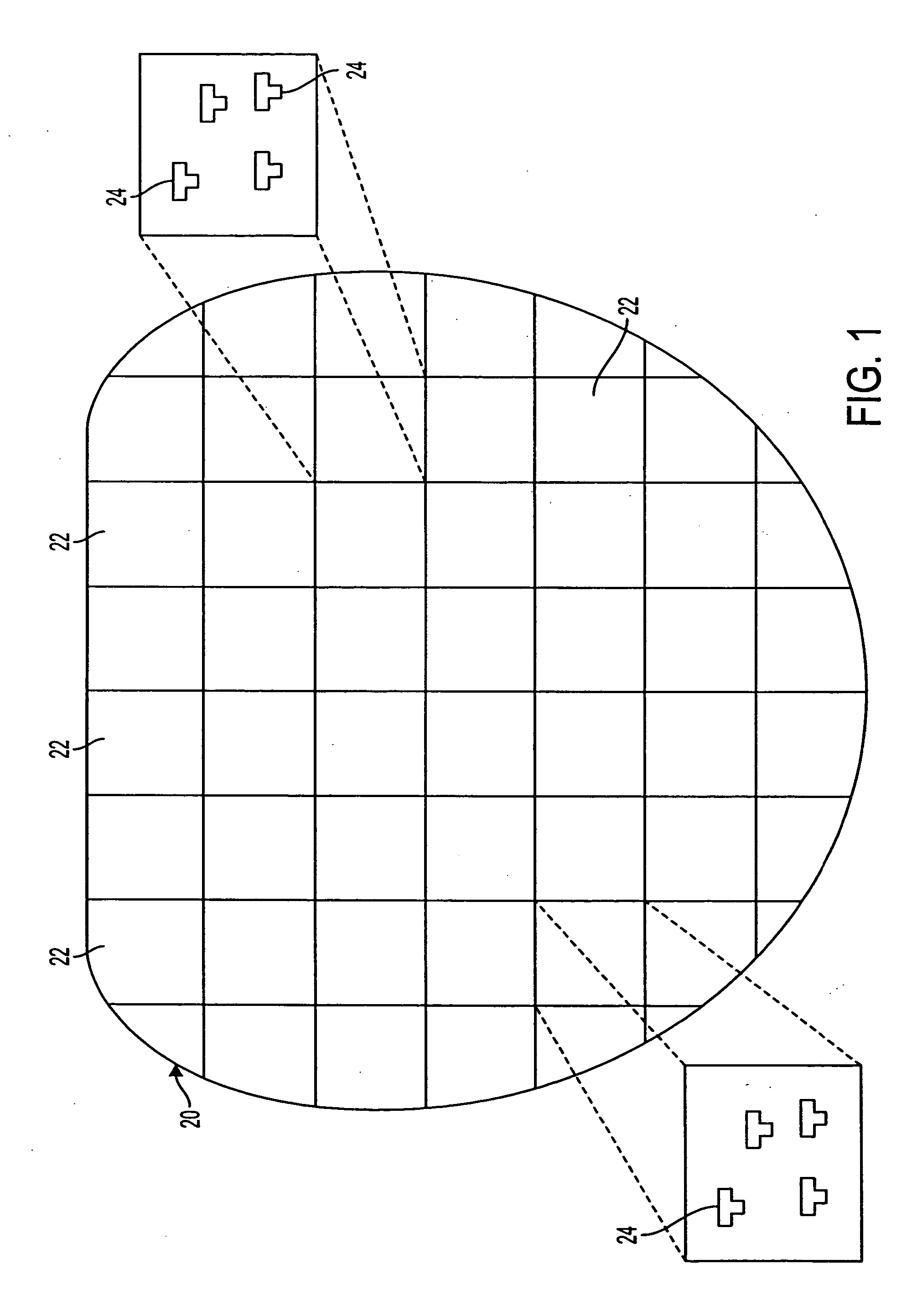
[0039] Referring to FIG. 1, an article to be inspected, such as a semiconductor wafer 20, is processed (prior to inspection) to have a plurality of ideally identical patterned integrated circuit dies 22, each die 22 having a comparable patterns, such as the T-shaped patterns 24 formed on the surface of wafer 20. It is noted that a single die may include a large amount of patterns that well exceed millions of patterns per die. A semiconductor die usually includes a plurality of layers. A pattern, such as local pattern 24 may be a part of a metal interconnection line, a trench, a via, a conductive gate, etc. It is noted that various areas on the die are usually categorized to background areas (that are ideally very smooth), memory areas (that include a large number of repetitive patterns) or logic areas (that usually do not include large quantities of adjacent repetitive patterns). It is noted that the method allows for dynamic definition of other categories / types and also for dynami...
PUM
| Property | Measurement | Unit |
|---|---|---|
| defects | aaaaa | aaaaa |
| threshold | aaaaa | aaaaa |
| noisy | aaaaa | aaaaa |
Abstract
Description
Claims
Application Information