Method for fabricating a memory cell

Inactive Publication Date: 2005-01-20
QIMONDA
View PDF18 Cites 22 Cited by
  • Summary
  • Abstract
  • Description
  • Claims
  • Application Information

AI Technical Summary

Benefits of technology

[0010] In the case of the method, after the fabrication of the gate dielectric and the gate electrode, a thin base layer, preferably made of oxide, is applied laterally with respect to the gate electrode. Silicon nanocrystals are then deposited onto the base layer. The silicon nanocrystals are covered with a thin covering layer, preferably an oxide. An auxiliary layer is deposited and removed to an extent such that the silicon nanocrystals present at the sidewalls of the gate electrode are accessible from above and can be etched back including the covering oxide. After

Problems solved by technology

In this case, however, the location of the charge stores is designed only by t

Method used


Image

  • Method for fabricating a memory cell
  • Method for fabricating a memory cell
  • Method for fabricating a memory cell

Examples


Embodiment Construction

[0019] The making and using of the presently preferred embodiments are discussed in detail below. It should be appreciated, however, that the present invention provides many applicable inventive concepts that can be embodied in a wide variety of specific contexts. The specific embodiments discussed are merely illustrative of specific ways to make and use the invention, and do not limit the scope of the invention.

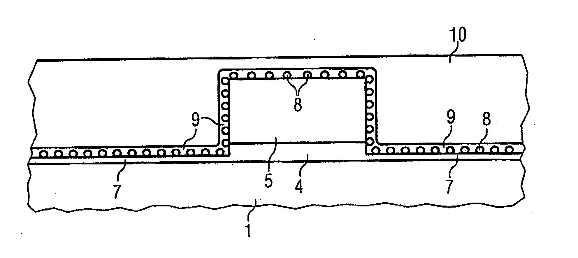
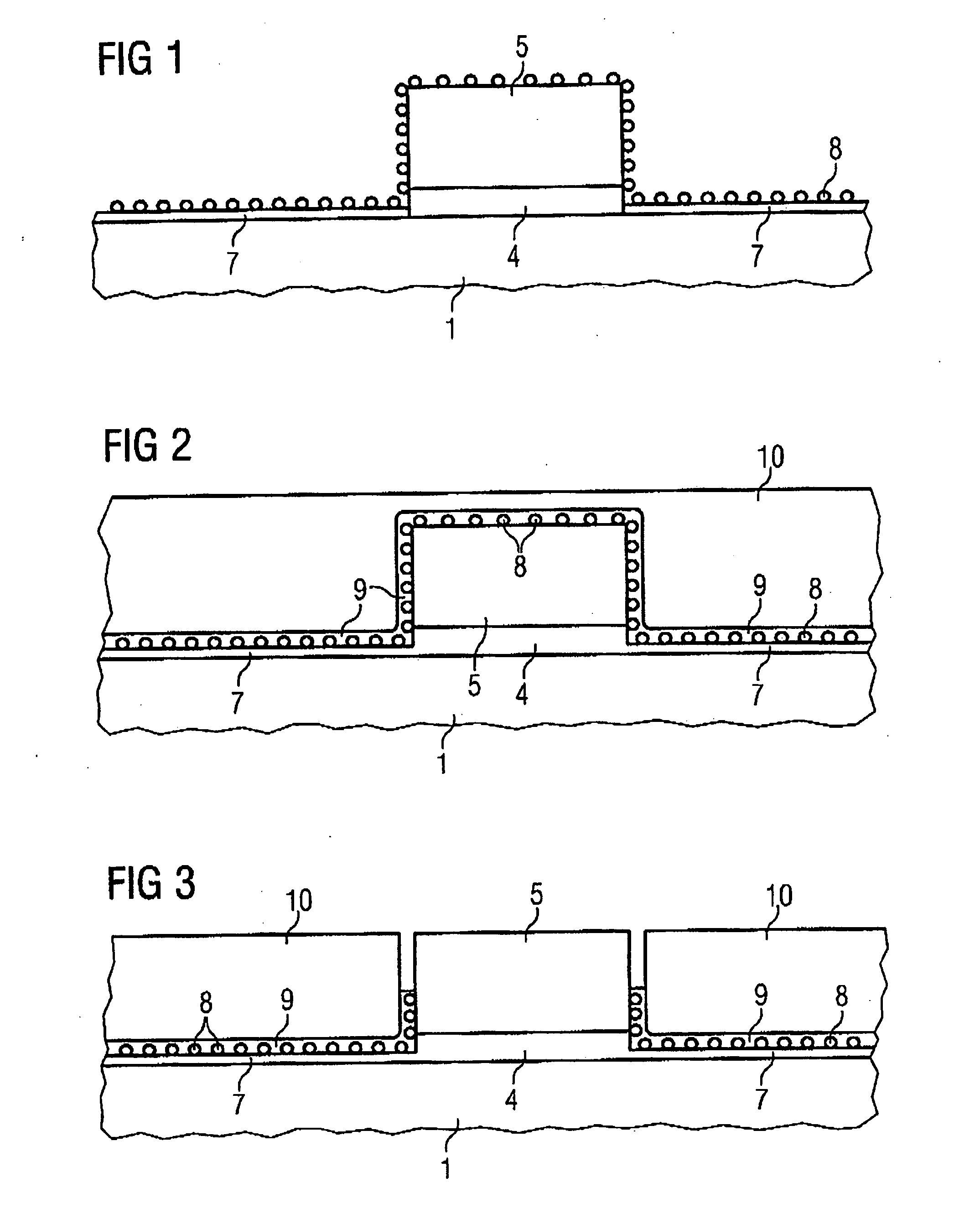
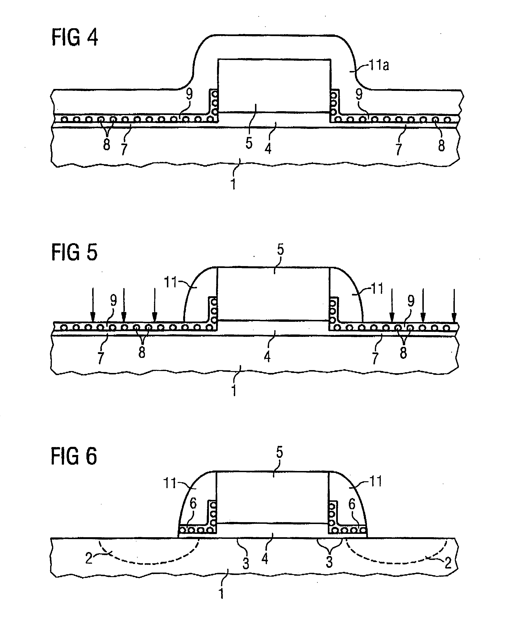
[0020] A description is given of a preferred fabrication method for an exemplary embodiment of the memory cell. FIG. 1 shows a cross-section through a semiconductor body 1 or a substrate made of semiconductor material. Between the memory cells or active areas, it is possible, as known per se, to fabricate trench isolations (e.g., STI, shallow trench isolation) or the like and to fabricate the doped wells provided for the memory transistors and the transistors of the driving periphery.

[0021] A thin layer of a gate dielectric 4 is then applied to the topside of the semicondu...


PUM


Abstract

Silicon nanocrystals are applied as storage layer (6) and removed using spacer elements (11) laterally with respect to the gate electrode (5). By means of an implantation of dopant, source/drain regions (2) are fabricated in a self-aligned manner with respect to the storage layer (6). The portions of the storage layer (6) are interrupted by the gate electrode (5) and the gate dielectric (4), so that a central portion of the channel region (3) is not covered by the storage layer (6). This memory cell is suitable as a multi-bit flash memory cell in a virtual ground architecture.

Description

[0001] This application claims priority to Germany Patent Application 103 26 805.7, which was filed Jun. 13, 2003 and is incorporated herein by reference. TECHNICAL FIELD [0002] The present invention relates generally to a memory device, and more particularly to a method for fabricating a memory cell. BACKGROUND [0003] U.S. Pat. No. 5,877,523 describes a semiconductor memory cell that is suitable for storing a plurality of bits. In the case of this cell, two floating gate electrodes separated from one another are situated at the ends of a channel region above two adjoining LDD regions of source and drain. A control gate electrode is present for driving purposes. Charges can be stored separately in the two floating gate electrodes in order to change the relevant programming state of the cell. In a central portion of the channel region, only the control gate electrode is situated above a dielectric layer on the semiconductor material. [0004] German Patent No. 100 36 911 C2 (also U.S. ...

Claims


Application Information

Patent Timeline
IPC IPC(8): H01L21/28H01L21/336H01L29/423H01L29/788
CPCB82Y10/00H01L21/28273H01L29/7887H01L29/66825H01L29/42332H01L29/40114
Inventor GOLDBACH, MATTHIASMIKOLAJICK, THOMASBIRNER, ALBERT
Owner QIMONDA
Why Eureka
Try Eureka