Semiconductor light-emitting device and method for manufacturing same

a technology of semiconductor light-emitting devices and semiconductors, which is applied in the direction of semiconductor devices, basic electric elements, electrical equipment, etc., can solve the problems of high accuracy and increase in cost, and achieve the effects of improving the light-emitting property of the resultant zn-base, improving the quality of the buffer layer, and raising the quality of the light-emitting region

Inactive Publication Date: 2005-01-27
SHIN-ETSU HANDOTAI CO LTD
View PDF1 Cites 50 Cited by
  • Summary
  • Abstract
  • Description
  • Claims
  • Application Information

AI Technical Summary

Benefits of technology

[0034] Use of the above-described fabrication method of this invention makes it possible to readily improve the quality of the buffer layer, and to raise the quality of the light emitting region. This consequently improves the light emitting property of the resultant Zn-base semiconductor light emitting device. In other words, the Zn-base semiconductor light emitting device of this invention is characterized by comprising at least a buffer layer containing an In-base compound or a Zn-base compound not contained in the substrate, and a light emitting region composed of a Zn-base compound, wherein the buffer layer is a polycrystal layer or an amorphous layer obtained after crystallization. As is known from the above, the buffer layer of the Zn-base semiconductor light emitting device of this invention comprises a polycrystal layer or an amorphous layer after being crystallized. The polycrystal layer or the amorphous layer herein to be subjected to the crystallization corresponds to the above-described precursory buffer layer, and the crystallization corresponds to the annealing for the above-described re-crystallization. This consequently makes it possible to readily and effectively improve the quality of the buffer layer as described in the above.

Problems solved by technology

The Zn-base semiconductor light emitting device is, however, fabricated by allowing a light emitting region composed of Zn-base semiconductor to epitaxially grow on the surface of a different kind of substrate such as a sapphire substrate, due to difficulty in obtaining a Zn-base semiconductor single crystal substrate having a desirable quality at low cost, unlike the case of a light emitting device using GaAs-base semiconductor or the like.
As is known from the above, formation of the stack to be converted into the buffer layer in a form of single crystal layer requires a high level of accuracy in the process control and causes increase in the cost.

Method used


Image

  • Semiconductor light-emitting device and method for manufacturing same
  • Semiconductor light-emitting device and method for manufacturing same
  • Semiconductor light-emitting device and method for manufacturing same

Examples


Embodiment Construction

[0043] The following paragraphs will describe best modes for carrying out this invention referring to the attached drawings.

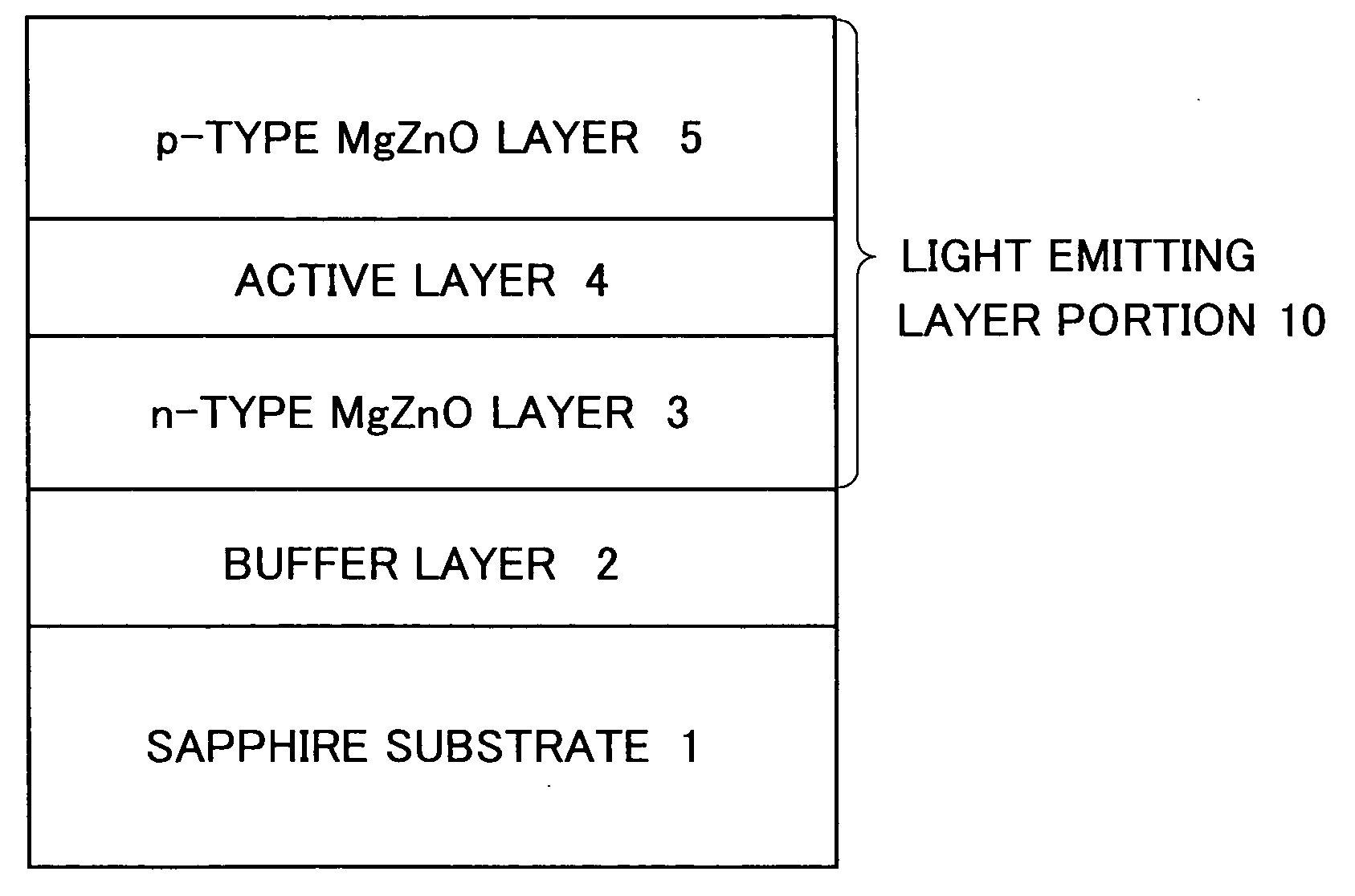
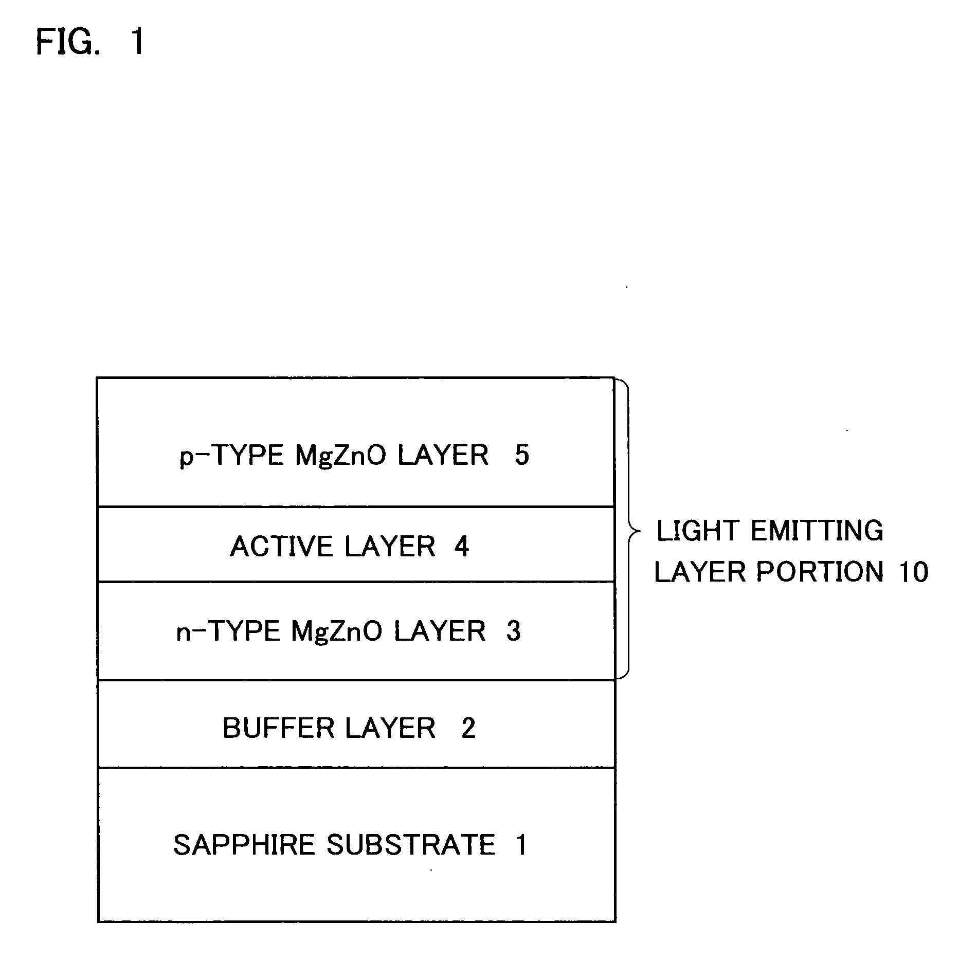
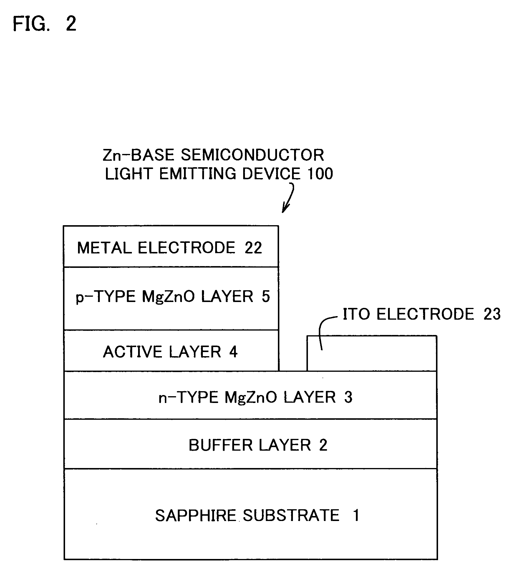
[0044]FIG. 1 is a schematic sectional view showing a stack structure of an essential portion of the Zn-base semiconductor light emitting device according to one embodiment of this invention. As shown in FIG. 1, a buffer layer 2 composed of ZnO is formed on the main surface of a sapphire substrate 1. An n-type MgZnO layer 3 composed of Mg1-aZnaO (0≦a≦1) (also referred to as MgZnO), an active layer 4 composed of a Zn-base compound, and a p-type MgZnO layer 5 are stacked in a lattice-matched manner by the epitaxial growth process to thereby form a light emitting layer portion 10 which serves as a double-hetero-type light emitting region. A material composing the active layer 4 is properly selected, for example, from ZnO, and ZnO-base materials having a part of Zn sites thereof substituted by Mg, or having a part of O sites thereof substituted by S, Se, Te or the ...


PUM


Abstract

On the surface of a substrate 1, a precursory buffer layer 2′ composed of an In-base compound or a Zn-base compound, not contained in the substrate 1, is formed so as to be stacked thereon as a polycrystal layer or an amorphous layer. Before a light emitting region is formed, the precursory buffer layer 2′ is annealed for re-crystallization to thereby convert it into a buffer layer 2. This successfully provides a Zn-base semiconductor light emitting device which can readily be fabricated and capable of improving quality of the light emitting region, and a method of fabricating the same.

Description

TECHNICAL FIELD [0001] This invention relates to a Zn-base semiconductor light emitting device and a method of fabricating the same. BACKGROUND ART [0002] ZnO (zinc oxide) is a direct-transition-type semiconductor having a band gap energy of 3.4 eV. A Zn-base semiconductor composed of ZnO or having ZnO as a base material is therefore a promising material for light emitting device capable of emitting light in blue to ultra-violet regions. The Zn-base semiconductor light emitting device is, however, fabricated by allowing a light emitting region composed of Zn-base semiconductor to epitaxially grow on the surface of a different kind of substrate such as a sapphire substrate, due to difficulty in obtaining a Zn-base semiconductor single crystal substrate having a desirable quality at low cost, unlike the case of a light emitting device using GaAs-base semiconductor or the like. For this reason, various efforts have been made on improvement in crystallinity of a buffer layer formed betw...

Claims


Application Information

Patent Timeline
Patent Type & Authority Applications(United States)
IPC IPC(8): H01L21/20H01L21/205H01L21/365H01L21/477H01L33/12H01L33/16H01L33/28
CPCH01L21/477H01L21/0262H01L33/0095H01L33/28H01L21/0242H01L21/02422H01L21/02472H01L21/02483H01L21/02513H01L21/02554H01L21/02565H01L21/02576H01L21/02579H01L21/02581H01L33/0087
Inventor ISHIZAKI, JUN-YA
Owner SHIN-ETSU HANDOTAI CO LTD
Why Eureka
Try Eureka