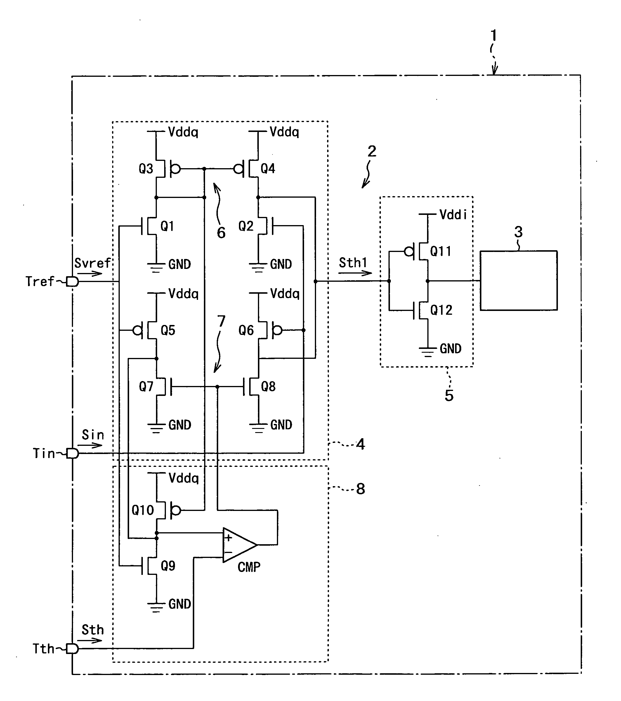
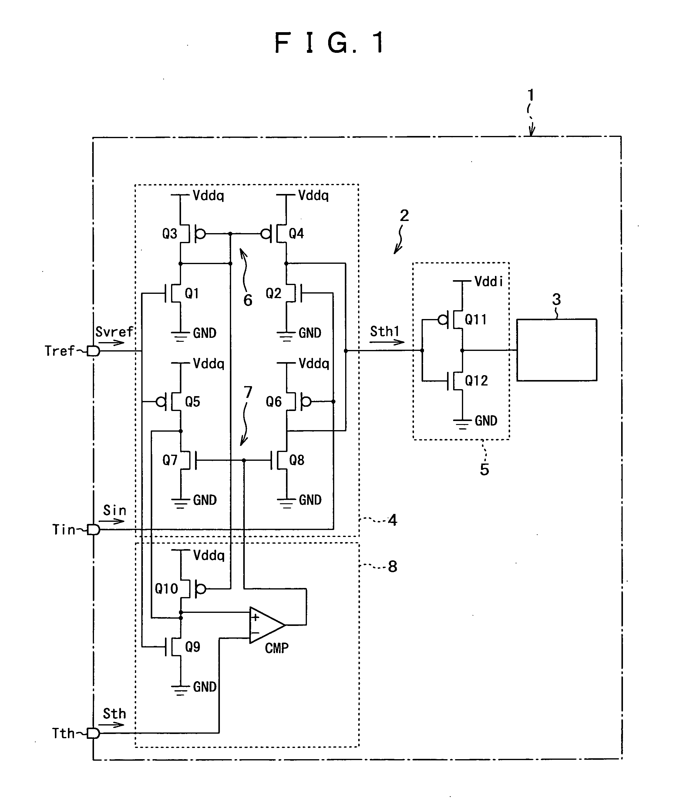
[0020] In this way, in the present invention, the output potential
control circuit is used to carry out the control so that, in
spite of the voltage value of the first drive voltage, the threshold of the output potential of the first buffer circuit becomes always the threshold of the input potential of the second buffer circuit. Thus, even if any variation is induced in the first drive voltage, the threshold of the output potential of the first buffer circuit and the threshold of the input potential of the second buffer circuit can be matched, and the erroneous operation of the second buffer circuit can be prevented, thereby normally operating the various circuits at the later stages, which are connected to the input buffer circuit.
[0022] And, when the output potential control circuit is configured so as to control the output potential of the first buffer circuit in accordance with one output potential of the pair of complementary
current mirror amplifiers constituting the first buffer circuit, the circuit configuration of the output potential control circuit can be made simpler, and regardless of the
simple circuit, the output potential of the first buffer circuit can be accurately controlled.
[0023] And, the present invention provides the following effects. That is, in the present invention according to the above first aspect, in the input buffer circuit in which the first and second buffer circuits operated at the first and second drive voltages whose voltages are different are connected in turn, it has the output potential control circuit for carrying out the control so that, in
spite of the voltage value of the first drive voltage, the threshold of the output potential of the first buffer circuit becomes the threshold of the input potential of the second buffer circuit. Thus, even if the variation is induced in the first drive voltage, the threshold of the output potential of the first buffer circuit and the threshold of the input potential of the second buffer circuit can be matched, and the erroneous operation of the second buffer circuit can be prevented, thereby normally operating the various circuits at the later stages, which are connected to the input buffer circuit.
[0024] Also, in the present invention according to the above second aspect, the output potential control circuit is configured such that the first buffer circuit is constituted by the pair of complementary current mirror amplifiers, and on the basis of the output potential on the reference side of this current mirror
amplifier, the generation of the output potential of the first buffer circuit is feedback-controlled. Thus, in spite of the potential of the input
signal, a
delay time can be kept constant, and regardless of the
simple circuit configuration, the output potential of the first buffer circuit can be accurately controlled.
[0025] Also, in the present invention according to the above third aspect, in the semiconductor apparatus having the input buffer circuit in which the first and second buffer circuits operated at the first and second drive voltages whose voltages are different are connected in turn, it has the output potential control circuit for carrying out the control so that, in spite of the voltage value of the first drive voltage, the threshold of the output potential of the first buffer circuit becomes the threshold of the input potential of the second buffer circuit. Thus, even if the variation is induced in the first drive voltage, the threshold of the output potential of the first buffer circuit and the threshold of the input potential of the second buffer circuit can be matched, and the erroneous operation of the second buffer circuit can be prevented, thereby operating the inner circuit of the semiconductor apparatus normally.
[0026] Also, in the present invention according to the above forth aspect, the output potential control circuit is configured such that the first buffer circuit is constituted by the pair of complementary current mirror amplifiers, and on the basis of the output potential on the reference side of this current mirror
amplifier, the generation of the output potential of the first buffer circuit is feedback-controlled. Thus, in spite of the potential of the input
signal, the
delay time can be kept constant, and regardless of the
simple circuit configuration, the output potential of the first buffer circuit can be accurately controlled, thereby improving the property of the semiconductor apparatus.

