

Drive circuit
a drive circuit and liquid crystal technology, applied in the direction of electric digital data processing, instruments, computing, etc., can solve the problems of obtaining the original effect of precharge operation, delay in switching timing between analog switch groups, etc., and achieve the effect of preventing overcurren
- Summary
- Abstract
- Description
- Claims
- Application Information
AI Technical Summary
Benefits of technology
Problems solved by technology
Method used
Image

Examples
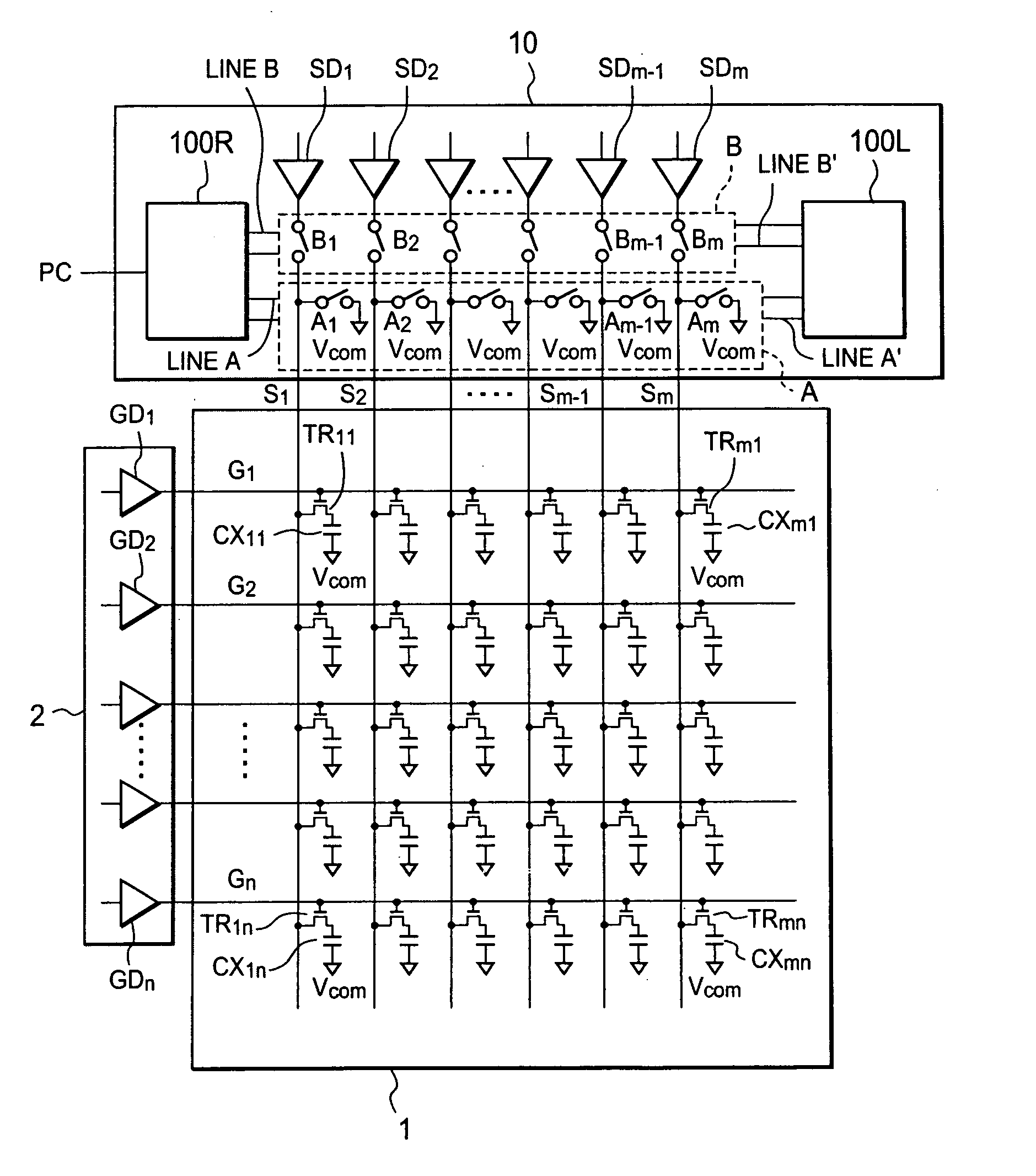
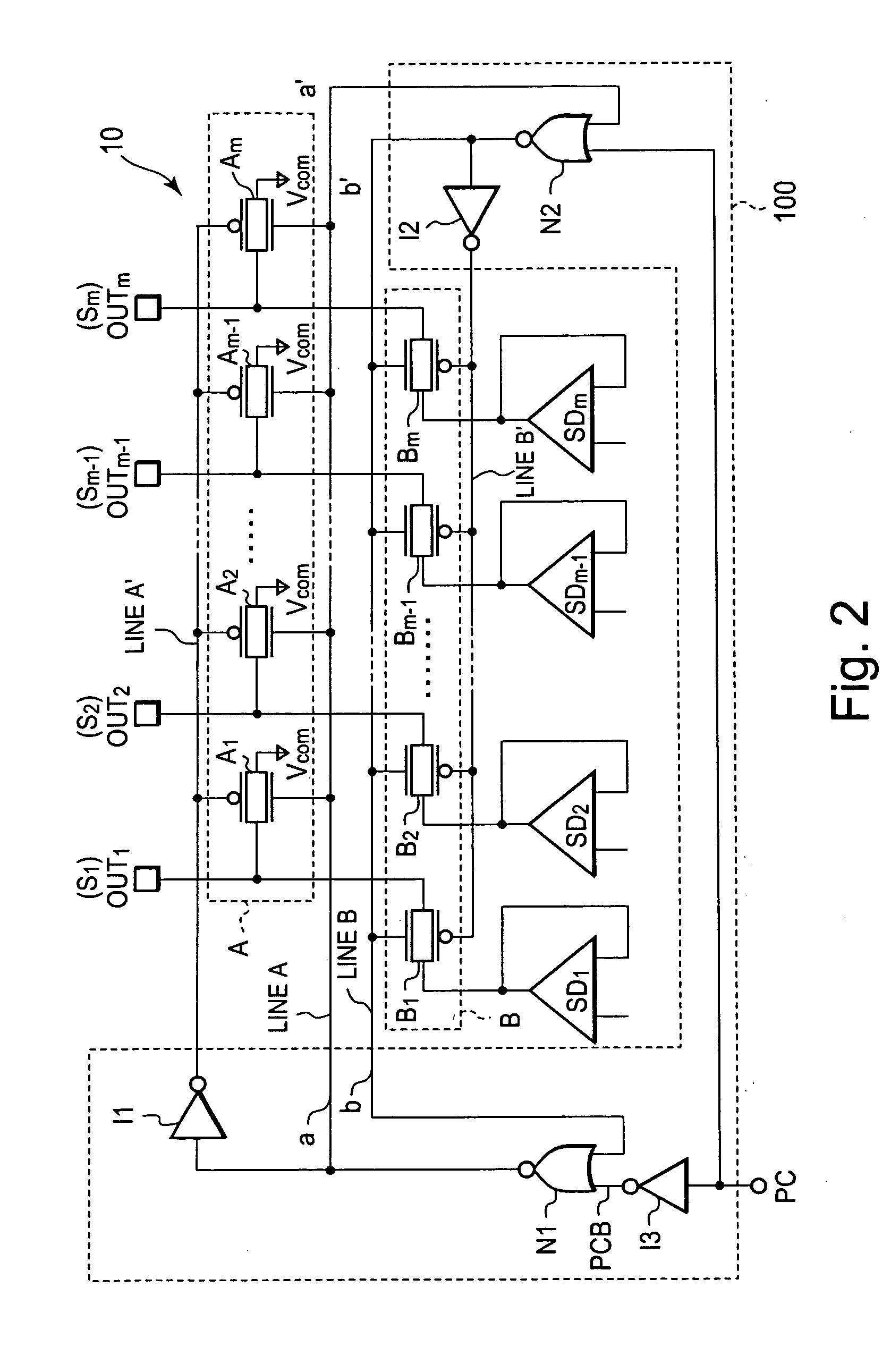
first embodiment
Operation of First Embodiment
[0063]FIG. 3 is a timing chart at 1-dot inversion driving of the source drive circuit 10 of the first embodiment of the present invention. In FIG. 3, reference numeral (1) indicates an output signal OUT (OUTi (Si) in FIG. 2) of the source drive circuit 10, reference numeral (2) indicates an input signal PC, reference numeral (3) indicates a signal PCB, reference numeral (4) indicates a wave form at point b and b′ of the signal line Line B, and reference numeral (5) indicates a wave form at point a and a′ of the signal line Line A, respectively. In addition, Td indicates a 1-dot period of the liquid crystal display, and Tp indicates a precharge period, respectively.
[0064]FIG. 4 is an enlarged view of the precharge period Tp in FIG. 3. In FIG. 4, reference numeral (1) indicates the input signal PC, reference numeral (2) indicates the signal PCB, reference numeral (3) indicates a wave form of the point b′ and b of the signal line LineB, and reference numer...
second embodiment
Operation of Second Embodiment
[0090]FIG. 7 is a timing chart at 2-dot inversion driving of the source drive circuit 20 of the second embodiment of the present invention. In FIG. 7, reference numeral (1) indicates an output signal OUT (OUTi (Si) in FIG. 6) of the source drive circuit 20, reference numeral (2) indicates an input signal LP, reference numeral (3) indicates an input signal PC, reference numeral (4) indicates a signal PCB, reference numeral (5) indicates a wave form at the points b′ and b of the signal line LineB, reference numeral (6) indicates a wave form at the point c (output of the NOR gate N1), and reference numeral (7) indicates wave form at the point a and a′ of the signal line LineA, respectively. Further, Td indicates a 1-dot period of the liquid crystal display, and Tp indicates a precharge period, respectively.
[0091]FIG. 8 is an enlarged view of the precharge period Tp in FIG. 7. In FIG. 8, reference numeral (1) indicates the input signal LP, reference numera...
third embodiment
[0115]FIG. 9 is a circuit configurational diagram showing a source drive circuit of a third embodiment of the present invention. Elements of structure similar to those shown in FIGS. 1 or 2 are respectively identified by the same reference numerals. The source drive circuit of the third embodiment includes a source driver group, an analog switch group A, an analog switch group B, and a switch control circuit 1000.
[0116] The switch control circuit 1000 shown in FIG. 9 is equivalent to the switch control circuit 100 (see FIGS. 1 and 2) of the first embodiment or the switch control circuit 200 (see FIGS. 5 and 6) of the second embodiment. The switch control circuit 1000 shown in FIG. 9 is divided into two elements so as to across the analog switch groups as described before. Therefore, in FIG. 9, a portion of the switch control circuit 1000 provided on the left side of the semiconductor chip is shown as a switch control circuit 1000L and a portion of the switch control circuit 1000 pr...
PUM
 Abstract
Description
Claims
Application Information