

Schottky Barrier Diode and Method for Using the Same
a barrier diode and diode technology, applied in the direction of semiconductor/solid-state device manufacturing, electrical apparatus, semiconductor devices, etc., can solve the problems of reducing yield and deteriorating performance of diodes, so as to prevent excess current, improve reverse-direction leakage current, and improve yield in mass production
Inactive Publication Date: 2009-10-01
CENTRAL RESEARCH INSTITUTE OF ELECTRIC POWER INDUSTRY
View PDF2 Cites 22 Cited by
- Summary
- Abstract
- Description
- Claims
- Application Information
AI Technical Summary
Benefits of technology
[0015]The Schottky barrier diode in accordance with the present invention reliably prevents an excess current during a forward operation and an increase in reverse-direction leak current caused by a pin-hole formed in the Schottky electrode. Consequently, a yield in a mass production can be improved.
[0016]According to the use of the Schottky barrier diode in accordance with the present invention, an excess current during a forward operation and an increase in reverse-direction leak current caused by a pin-hole formed in the Schottky electrode can be reliably prevented.
Problems solved by technology
Such a diode having a deteriorated performance cannot be shipped as a product, thereby reducing a yield.
Method used
View moreImage
Smart ImageViewing Examples

Examples
example 1
[0041]Schottky electrode: Ti (work function: 4.33 eV)
Intermediate metal film: Ni (work function: 5.15 eV)
Pad electrode: Al (work function: 4.28 eV)<
example 2
[0042]Schottky electrode: W (work function: 4.55 eV)
Intermediate metal film: Ni (work function: 5.15 eV)
Pad electrode: Al (work function: 4.28 eV)<
example 3
[0043]Schottky electrode: Ti (work function: 4.33 eV)
Intermediate metal film: Ni (work function: 5.15 eV)
Pad electrode: Mo (work function: 4.6 eV)<
Login to View More PUM
| Property | Measurement | Unit |
|---|---|---|
| thickness | aaaaa | aaaaa |
| thickness | aaaaa | aaaaa |
| thickness | aaaaa | aaaaa |
Abstract
An intermediate metal film is formed between a Schottky electrode and a pad electrode. A Schottky barrier height between the intermediate metal film and a silicon carbide epitaxial film is equivalent to or higher than a Schottky barrier height between the Schottky electrode and the silicon carbide epitaxial film. By this configuration, an excess current and a leak current through a pin-hole can be suppressed even in the case in which a Schottky barrier height between the pad electrode and the silicon carbide epitaxial film is less than the Schottky barrier height between the Schottky electrode and the silicon carbide epitaxial film.
Description
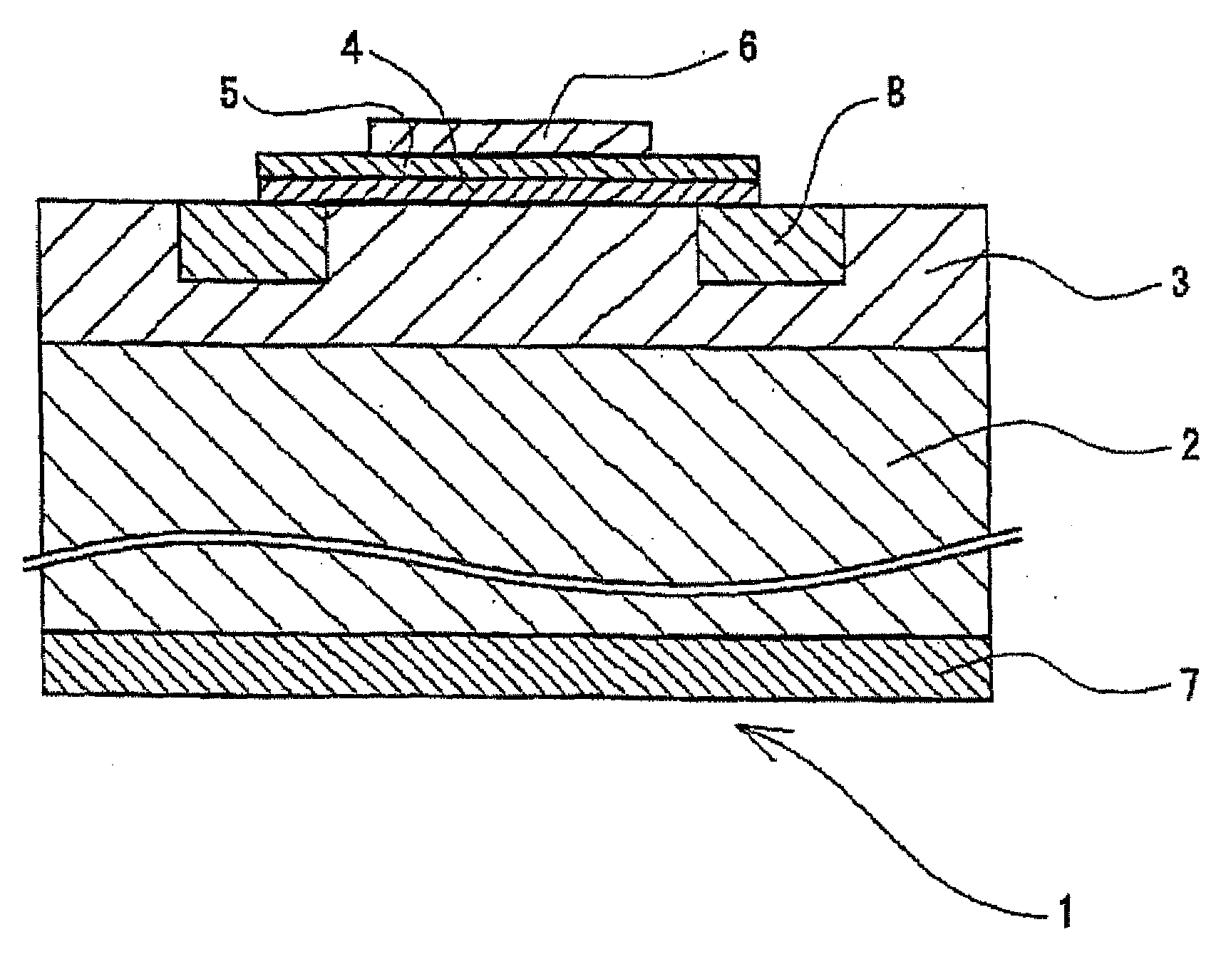
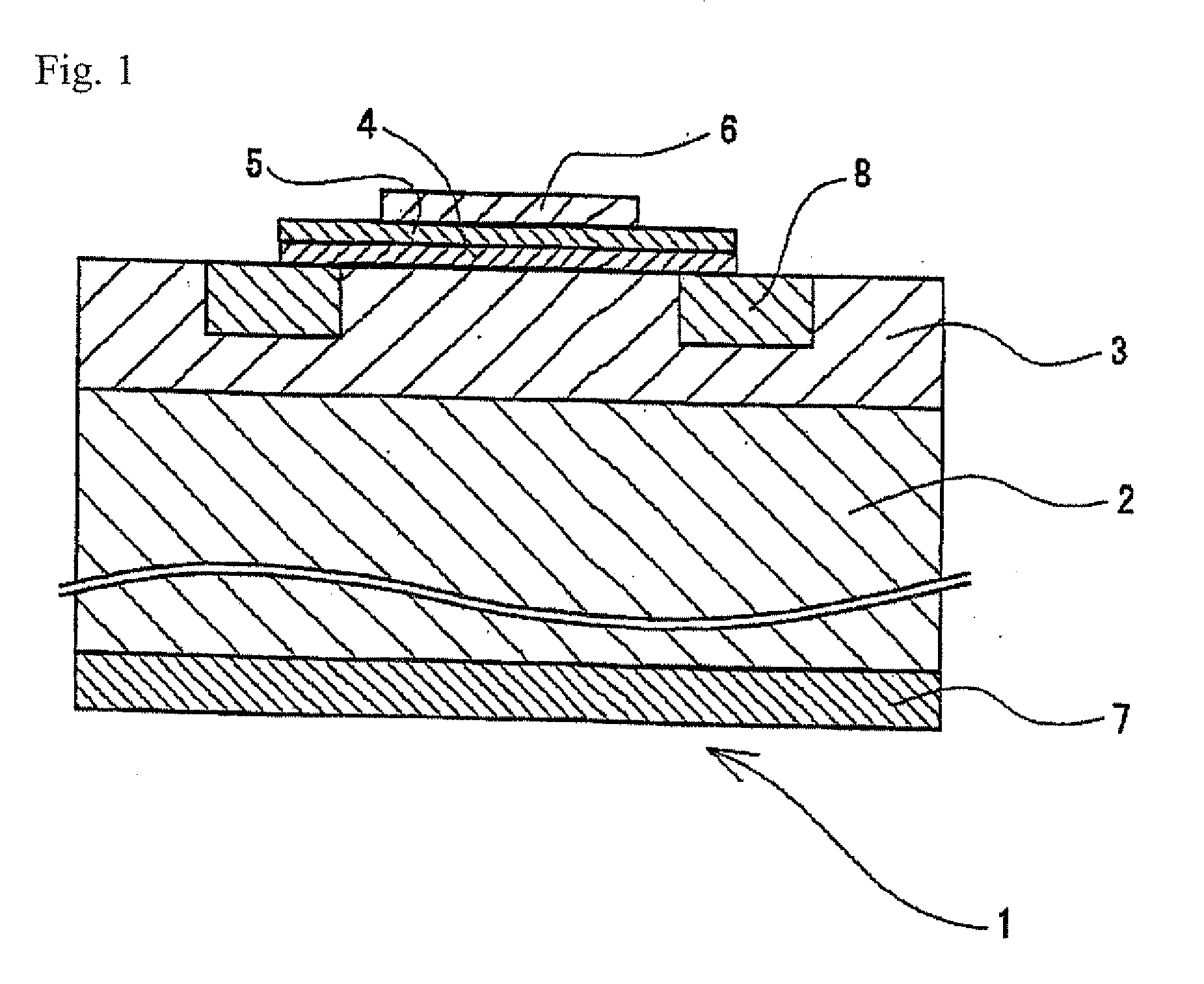
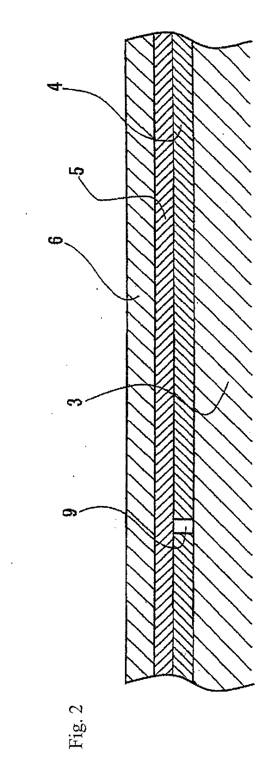
TECHNICAL FIELD[0001]The present invention relates to a Schottky barrier diode and use of the Schottky barrier diode. More specifically, the present invention relates to a Schottky barrier diode in which a Schottky electrode is formed on the surface of a silicon carbide epitaxial film grown from the surface of a silicon carbide single-crystal substrate and in which a pad electrode for being electrically connected to the outside is formed on the Schottky electrode.BACKGROUND ART[0002]Silicon carbide (SiC) is a wide gap semiconductor having excellent physical properties such as an approximately triple band gap, an approximately double saturated drift velocity, and an approximately decuple dielectric breakdown field strength as compared with silicon (Si). Consequently, silicon carbide has been developed as a material of a power semiconductor device, and Schottky barrier diodes manufactured by using SiC have been on the market.[0003]FIG. 3 is a cross-sectional view showing a conventiona...
Claims
Login to View More Application Information
Patent Timeline
 Patent Type & AuthorityApplications(United States)
IPC IPC(8): H01L29/872
CPCH01L29/0615H01L29/1608H01L29/872H01L29/6606H01L29/47
InventorNAKAMURA, TOMONORITSUCHIDA, HIDEKAZUMIYANAGI, TOSHIYUKI
OwnerCENTRAL RESEARCH INSTITUTE OF ELECTRIC POWER INDUSTRY