Nanoscale digital data storage device

a digital data and storage device technology, applied in the field of data storage devices, can solve the problems of data storage devices that are not able to meet mass production, data recording devices are very complex in structure, data storage devices are infeasible for mass production, etc., and achieve the effect of improving energy efficiency

Inactive Publication Date: 2005-01-27
SAMSUNG ELECTRONICS CO LTD
View PDF9 Cites 20 Cited by
  • Summary
  • Abstract
  • Description
  • Claims
  • Application Information

AI Technical Summary

Benefits of technology

[0010] It is another object of the present invention to provide a nanoscale digital data storage device with a significantly improved energy efficiency.

Problems solved by technology

A drawback of this writing mechanism is that the data storage device is very complex in structure to forcibly move or transform each cantilever.
The resulting high cost and low stability render the data storage device infeasible for mass production.
Moreover, heating the overall surface of the storage medium before writing is not preferable in terms of energy efficiency.

Method used


Image

  • Nanoscale digital data storage device
  • Nanoscale digital data storage device
  • Nanoscale digital data storage device

Examples


Embodiment Construction

[0032] Preferred embodiments of the present invention will be described herein below with reference to the accompanying drawings. In the following description, well-known functions or constructions are not described in detail since they would obscure the invention in unnecessary detail.

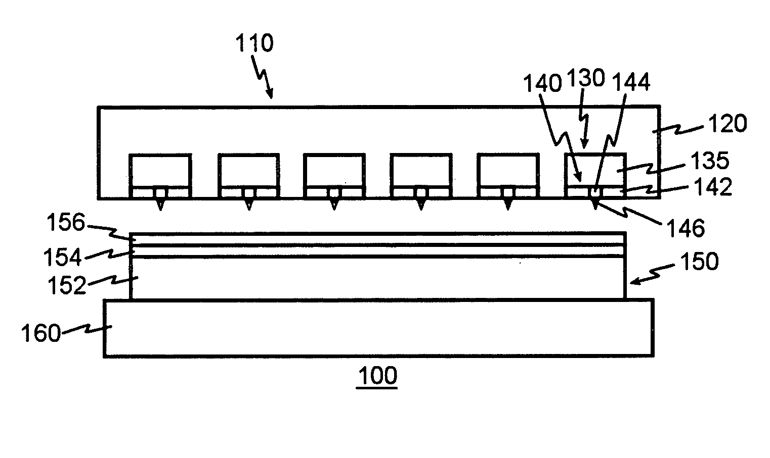
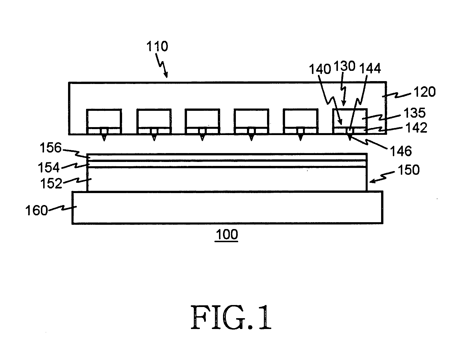
[0033]FIG. 1 illustrates a nanoscale digital storage device according to an embodiment of the present invention. Referring to FIG. 1, the storage device 100 includes a cantilever chip 110, a storage medium 150, and a stage 160.

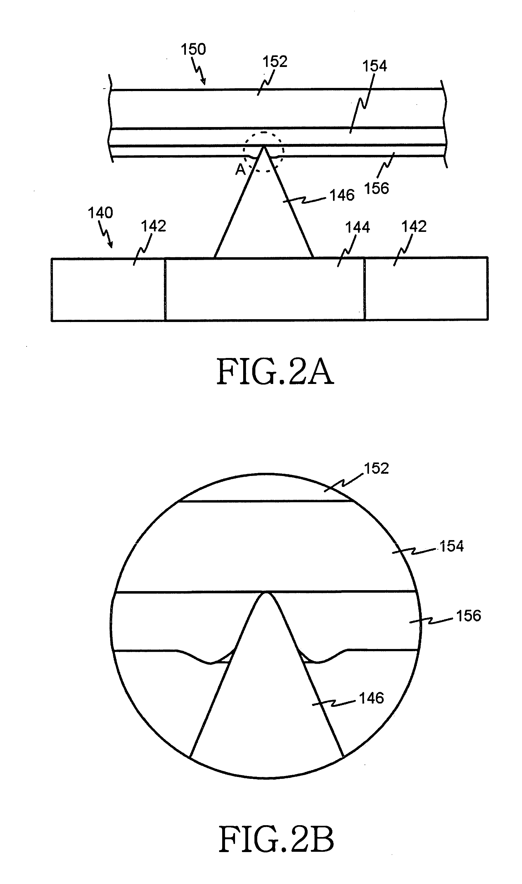
[0034] The cantilever chip 110 has a plurality of cantilever cells 130 arranged in a matrix. Each of the cantilever cells 130 writes or reads one-bit digital data “1” or “0” on or from the storage medium 150. The cantilever cell 130 includes a cantilever 140 and an underlying empty space 135. The cantilever 140 is comprised of an electrically resistive platform 144 and legs 142 for connecting the platform 144 to a substrate 120. For digital data writing and reading, all tips 1...


PUM

PropertyMeasurementUnit
sizeaaaaaaaaaa
threshold temperatureaaaaaaaaaa
sizeaaaaaaaaaa

Abstract

A nanoscale digital data storage device is provided. In the nanoscale digital data storage device, a storage medium has a polymer layer deposited on a substrate, for writing and reading digital data on and from. A cantilever chip has a plurality of cantilevers arranged therein. Each cantilever is fixed to another substrate at one end and has a tip formed at its free end, for emitting heat according to an applied current. The tips in the cantilever chip are in contact with the storage medium at predetermined bit positions during data writing, and the cantilever chip applies a relatively low current to a tip when the tip writes bit 1 and a relatively high current to the tip when the tip writes bit 0.

Description

PRIORITY [0001] This application claims priority under 35 U.S.C. § 119 to an application entitled “Nanoscale Digital Data Storage Device” filed in the Korean Intellectual Property Office on Jul. 23, 2003 and assigned Serial No. 2003-50628, the contents of which are incorporated herein by reference. BACKGROUND OF THE INVENTION [0002] 1. Field of the Invention [0003] The present invention relates generally to a data storage device, and in particular, to a nanoscale digital data storage device for writing and reading data by mechanical contact. [0004] 2. Description of the Related Art [0005] Thomas R. Albrecht, et. al. proposed a data storage system using a cantilever having a tip in U.S. Pat. No. 5,537,372 entitled “High Density Data Storage System with Topographic Contact Sensor”. In the data storage system, the tip physically contacts the surface of a storage medium and the medium has pits representing mechanically readable data on its surface. During a read operation, a change of t...

Claims


Application Information

Patent Timeline
Patent Type & Authority Applications(United States)
IPC IPC(8): G11B9/00
CPCB82Y10/00G11B9/14G11B9/1409G11B9/1418G11B11/007G11B2005/0021G11B9/1472G11B9/149G11B9/1445
Inventor PETRIN, ANDREI B.
Owner SAMSUNG ELECTRONICS CO LTD
Why Eureka
Try Eureka