Substrate treating method and apparatus
a technology of substrate and treatment method, applied in the direction of liquid surface applicators, pretreated surfaces, coatings, etc., can solve the problems of increasing the operating speed of circuits, increasing the leak current due to the thin film, and reaching the limit of gate insulating oxide film thin formation, etc., to achieve effective treatment
- Summary
- Abstract
- Description
- Claims
- Application Information
AI Technical Summary
Benefits of technology
Problems solved by technology
Method used
Image

Examples
first embodiment
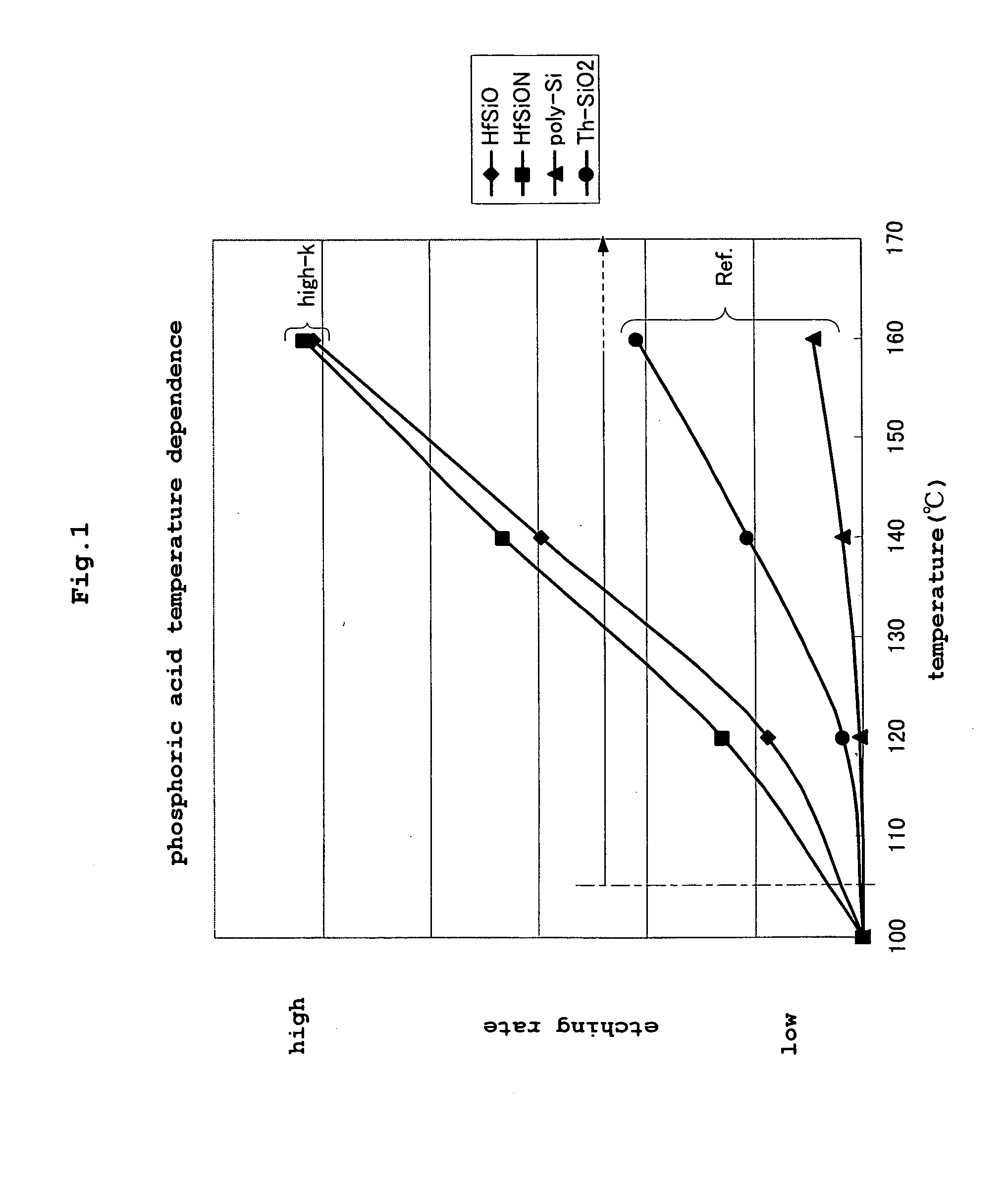
[0041]FIG. 1 is a graph showing results of an experiment conducted with a method in a first embodiment of this invention, which shows a temperature dependence of etching rate.
[0042] This graph is a graphic representation of etching rates which are results of an experiment conducted in etching substrates coated with a film including a material of high dielectric constant. The etching process was carried out by using, as an etching solution, a treating solution containing phosphoric acid. The solution was heated to varied temperatures, and the etching rate was measured at the varied temperatures. Specifically, the treating solution was heated to 100° C., 120° C., 140° C. and 160° C. The concentration of phosphoric acid in the treating solution was about 90% by weight.
[0043] Substrates coated with a film including hafnium Hf which is a material of high dielectric constant were used as samples in the experiment. And polysilicon and thermal oxidation film as used in the prior art were ...
second embodiment
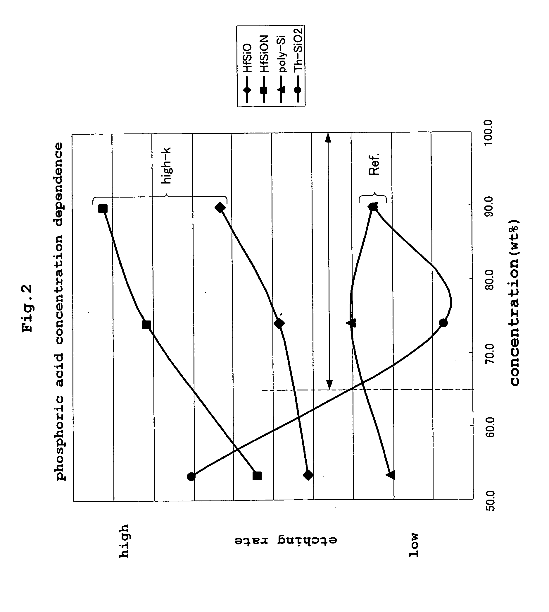
[0062]FIG. 5 is a graph showing results of an experiment conducted with a method in a second embodiment of this invention, which shows a sulfuric acid concentration dependence of etching rate.
[0063] This graph is a graphic representation of etching rates which are results of an experiment conducted in etching substrates coated with a film including a material of high dielectric constant. The etching process was carried out by using a treating solution containing phosphoric acid and sulfuric acid, and the etching rate was measured while varying sulfuric acid concentration. Specifically, a mixing ratio between phosphoric acid and sulfuric acid (a weight ratio of sulfuric acid to phosphoric acid) was varied to 0% by weight, 25% by weight, 50% by weight and 75% by weight. The temperature of the treating solution was 120° C. which was in the temperature range noted in the first embodiment. The samples used in this experiment are the same as those in the first embodiment.
[0064] As seen ...
PUM
| Property | Measurement | Unit |
|---|---|---|
| temperature | aaaaa | aaaaa |
| dielectric constant | aaaaa | aaaaa |
| boiling point | aaaaa | aaaaa |
Abstract
Description
Claims
Application Information
 - R&D
- Intellectual Property
- Life Sciences
- Materials
- Tech Scout
- Unparalleled Data Quality
- Higher Quality Content
- 60% Fewer Hallucinations
Browse by: Latest US Patents, China's latest patents, Technical Efficacy Thesaurus, Application Domain, Technology Topic, Popular Technical Reports.
© 2025 PatSnap. All rights reserved.Legal|Privacy policy|Modern Slavery Act Transparency Statement|Sitemap|About US| Contact US: help@patsnap.com