
Apparatus and method for managing memory defects

a memory defect and apparatus technology, applied in the field of high-performance switching, can solve the problems of increasing design requirements, increasing design constraints, and relatively slow conventional dynamic random access memory (dram)

Inactive Publication Date: 2005-01-27
AVAGO TECH WIRELESS IP SINGAPORE PTE
View PDF8 Cites 11 Cited by
  • Summary
  • Abstract
  • Description
  • Claims
  • Application Information

AI Technical Summary

Problems solved by technology

As speed has increased, design constraints and design requirements have become more and more complex with respect to following appropriate design and protocol rules and providing a low cost, commercially viable solution.
For example, high speed switching requires high speed memory to provide appropriate buffering of packet data; conventional Dynamic Random Access Memory (DRAM) is relatively slow, and requires hardware-driven refresh.
The speed of DRAMs, therefore, as buffer memory in network switching, results in valuable time being lost, and it becomes almost impossible to operate the switch or the network at linespeed.
Additionally, as network switches have become more and more complicated with respect to requiring rules tables and memory control, a complex multi-chip solution is necessary which requires logic circuitry, sometimes referred to as glue logic circuitry, to enable the various chips to communicate with each other.
Additionally, cost / benefit tradeoffs are necessary with respect to expensive but fast SRAMs versus inexpensive but slow DRAMs.

Method used


Image

  • Apparatus and method for managing memory defects
  • Apparatus and method for managing memory defects
  • Apparatus and method for managing memory defects

Examples


Embodiment Construction

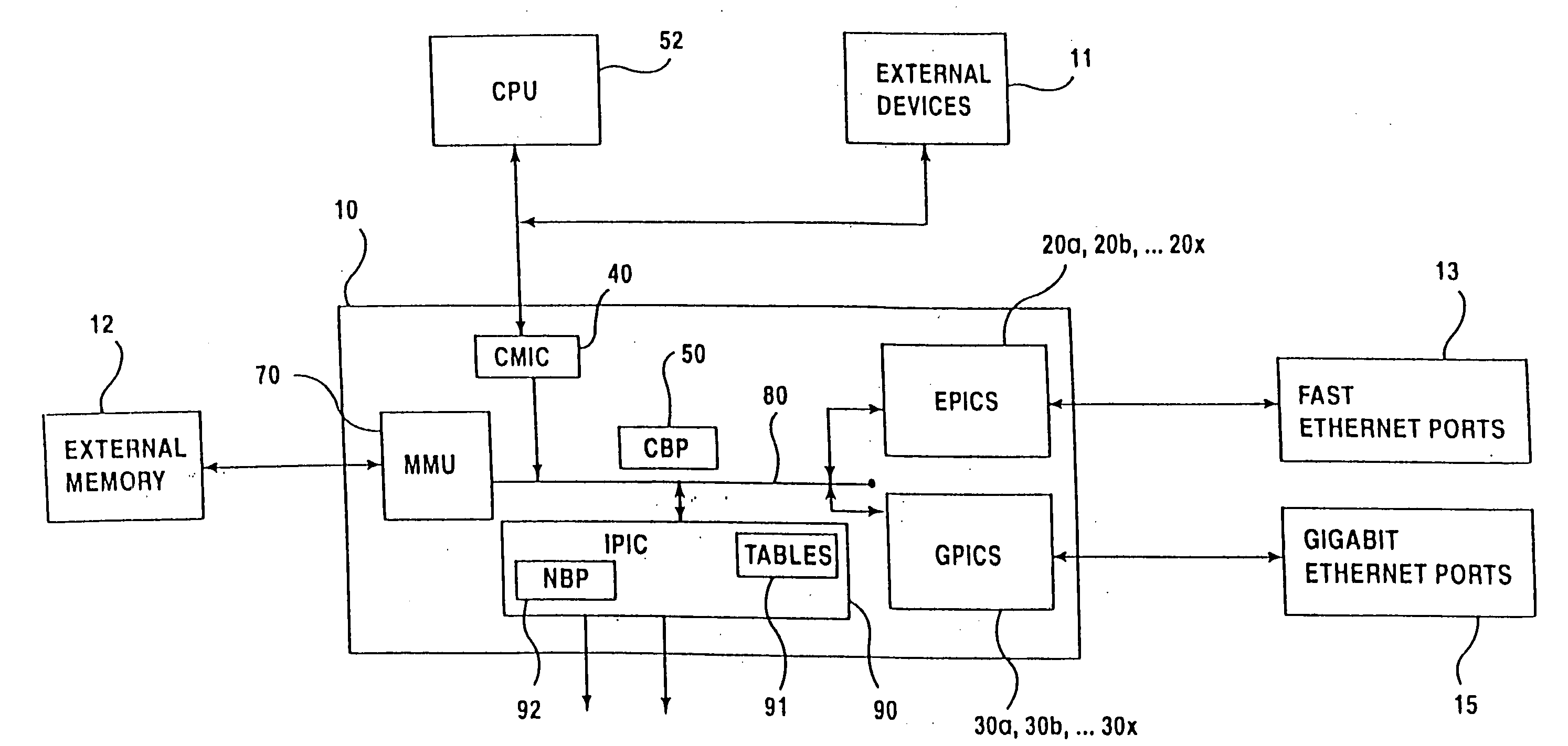
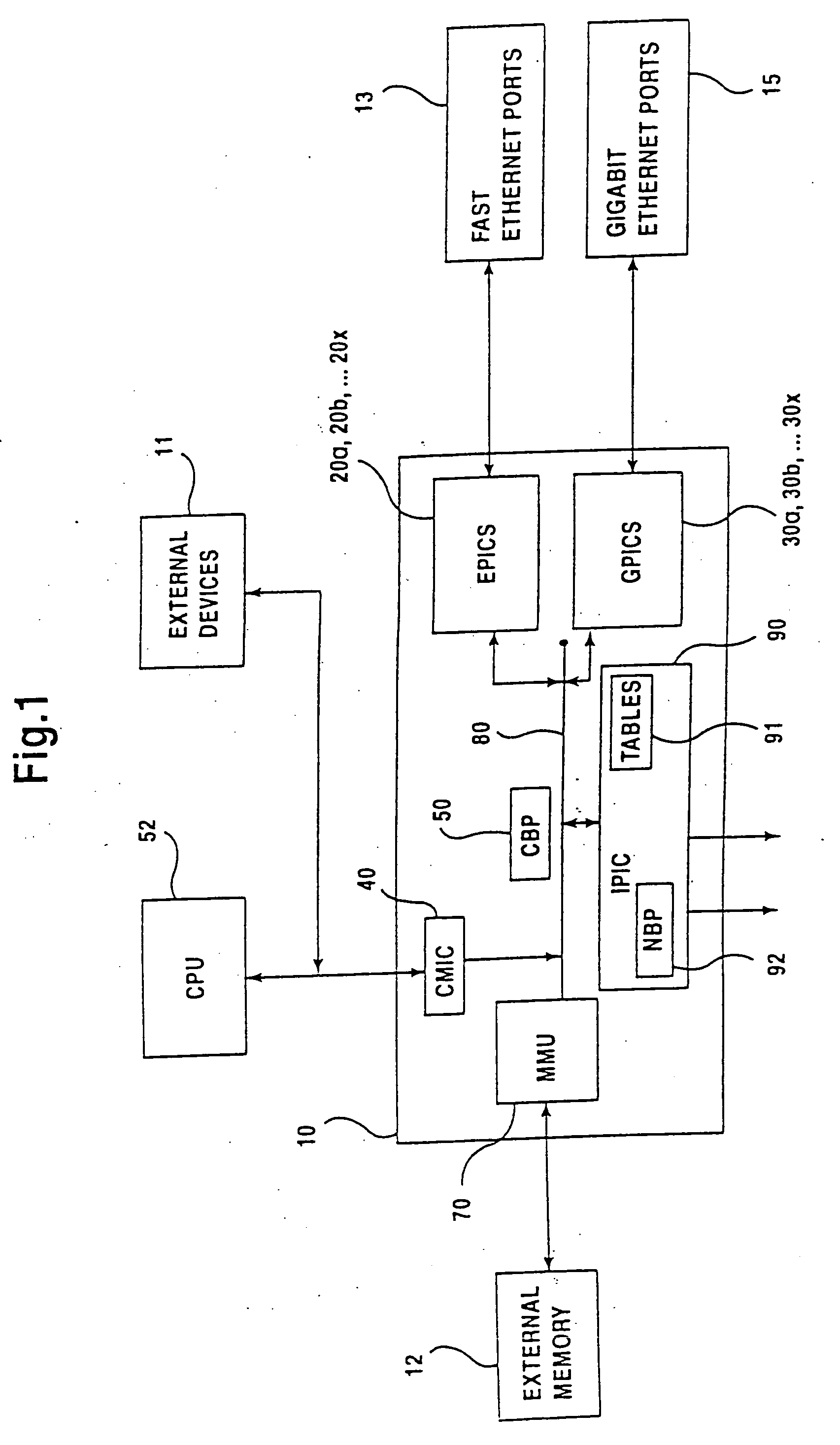
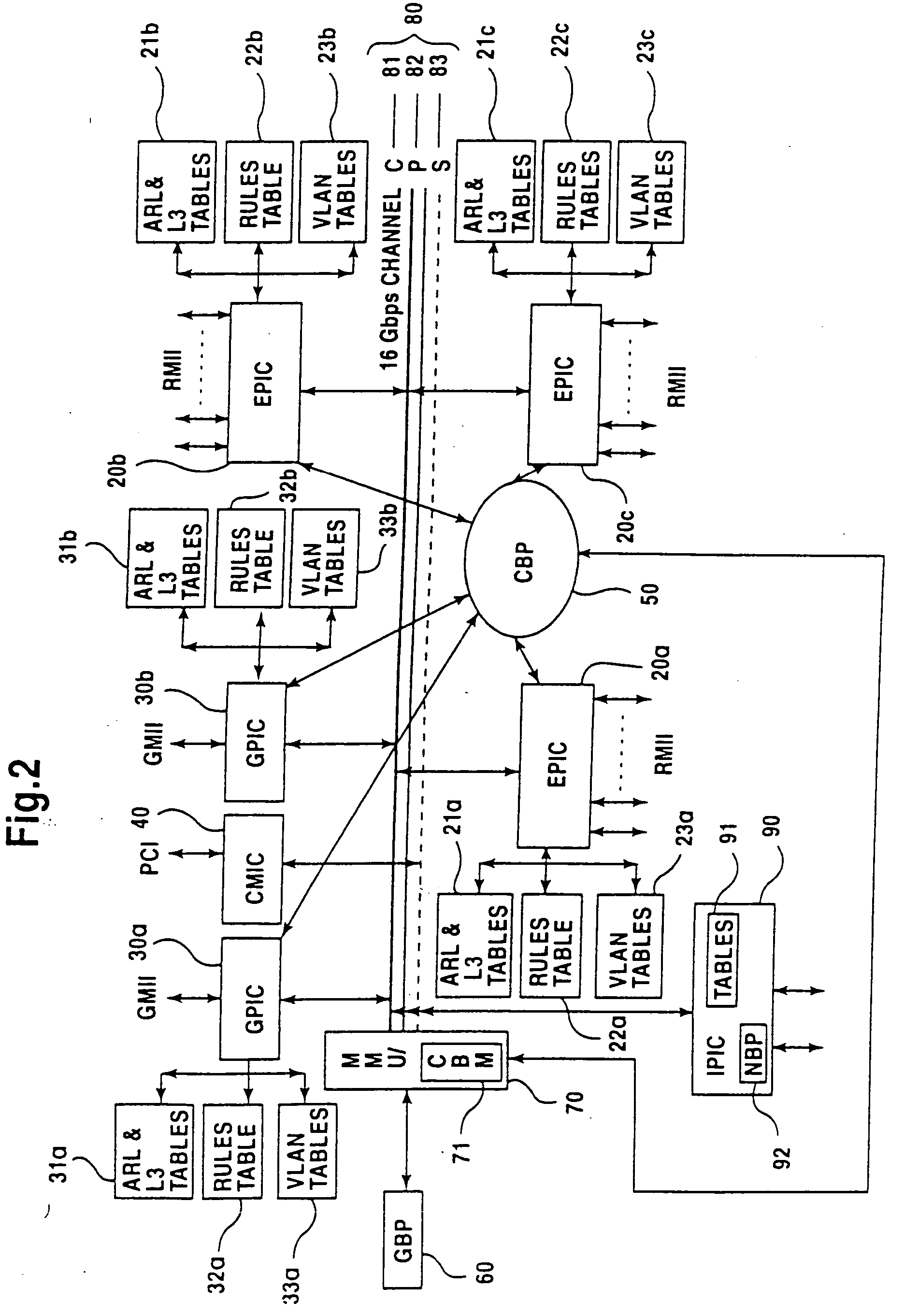
FIG. 1 illustrates a configuration wherein a switch-on-chip (SOC) 10, in accordance with the present invention, is functionally connected to external devices 11, external memory 12, fast ethernet ports 13, and gigabit ethernet ports 15. For the purposes of this embodiment, fast ethernet ports 13 will be considered low speed ethernet ports, since they are capable of operating at speeds ranging from 10 Mbps to 100 Mbps, while the gigabit ethernet ports 15, which are high speed ethernet ports, are capable of operating at 1000 Mbps. External devices 11 could include other switching devices for expanding switching capabilities, or other devices as may be required by a particular application. External memory 12 is additional off-chip memory, which is in addition to internal memory which is located on SOC 10, as will be discussed below. CPU 52 can be used as necessary to program SOC 10 with rules which are appropriate to control packet processing. However, once SOC 10 is appropriately prog...


PUM


Abstract

A method and apparatus for managing defects in a memory, wherein the method includes the steps of testing a plurality of memory locations to determine an inoperable memory location and moving a memory address corresponding to the inoperable memory location to a first position in a list of available memory addresses. The method further includes the steps of incrementing an address pointer to a second position in the list of available addresses indicating a next available memory address in the list of available addresses, wherein said step of incrementing an address pointer to a second position operates to remove the memory address stored in the first position from the list of available memory addresses. The apparatus includes a memory having a predetermined number of memory locations for storing data and an address pool having a predetermined number of available memory addresses therein, each of said predetermined number of available addresses corresponding to one of the predetermined number of memory locations. An address pool controller is provided, wherein the address pool controller manages defects in the memory by removing an address from the predetermined number of available addresses when the address is identified as corresponding to an inoperable memory location.

Description

BACKGROUND OF THE INVENTION 1. Field of the Invention The invention relates to a method and apparatus for high performance switching in local area communications networks such as token ring, ATM, ethernet, fast ethernet, and gigabit ethernet environments, generally known as LANs. In particular, the invention relates to a new switching architecture in an integrated, modular, single chip solution, which can be implemented on a semiconductor substrate such as a silicon chip. 2. Description of the Related Art As computer performance has increased in recent years, the demands on computer networks has significantly increased; faster computer processors and higher memory capabilities need networks with high bandwidth capabilities to enable high speed transfer of significant amounts of data. The well-known ethernet technology, which is based upon numerous IEEE ethernet standards, is one example of computer networking technology which has been able to be modified and improved to remain a...

Claims


Application Information

Patent Timeline
IPC IPC(8): H04L12/56H04L29/06H04Q11/04
CPCH04L12/56H04L69/16H04Q11/0478
Inventor HERBST, JOSEPH
Owner AVAGO TECH WIRELESS IP SINGAPORE PTE
Learn More