Electro-optic sensor

a sensor and optical technology, applied in the field of optical sensors, can solve the problem of inherently inefficient confirmation between process steps

Active Publication Date: 2005-02-03
LER TECH
View PDF4 Cites 75 Cited by
  • Summary
  • Abstract
  • Description
  • Claims
  • Application Information

AI Technical Summary

Problems solved by technology

A measurement technique that delays the process awaiting measurement

Method used


Image

  • Electro-optic sensor
  • Electro-optic sensor
  • Electro-optic sensor

Examples


Embodiment Construction

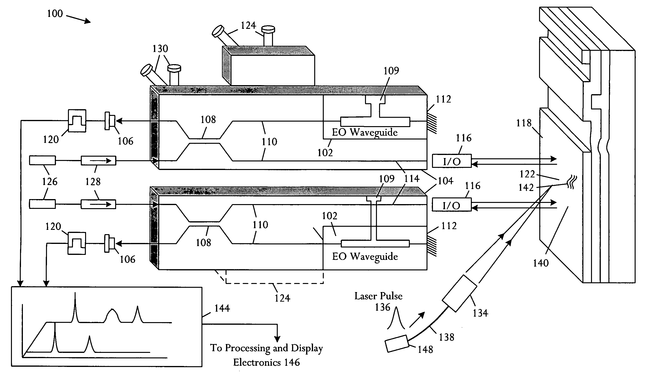
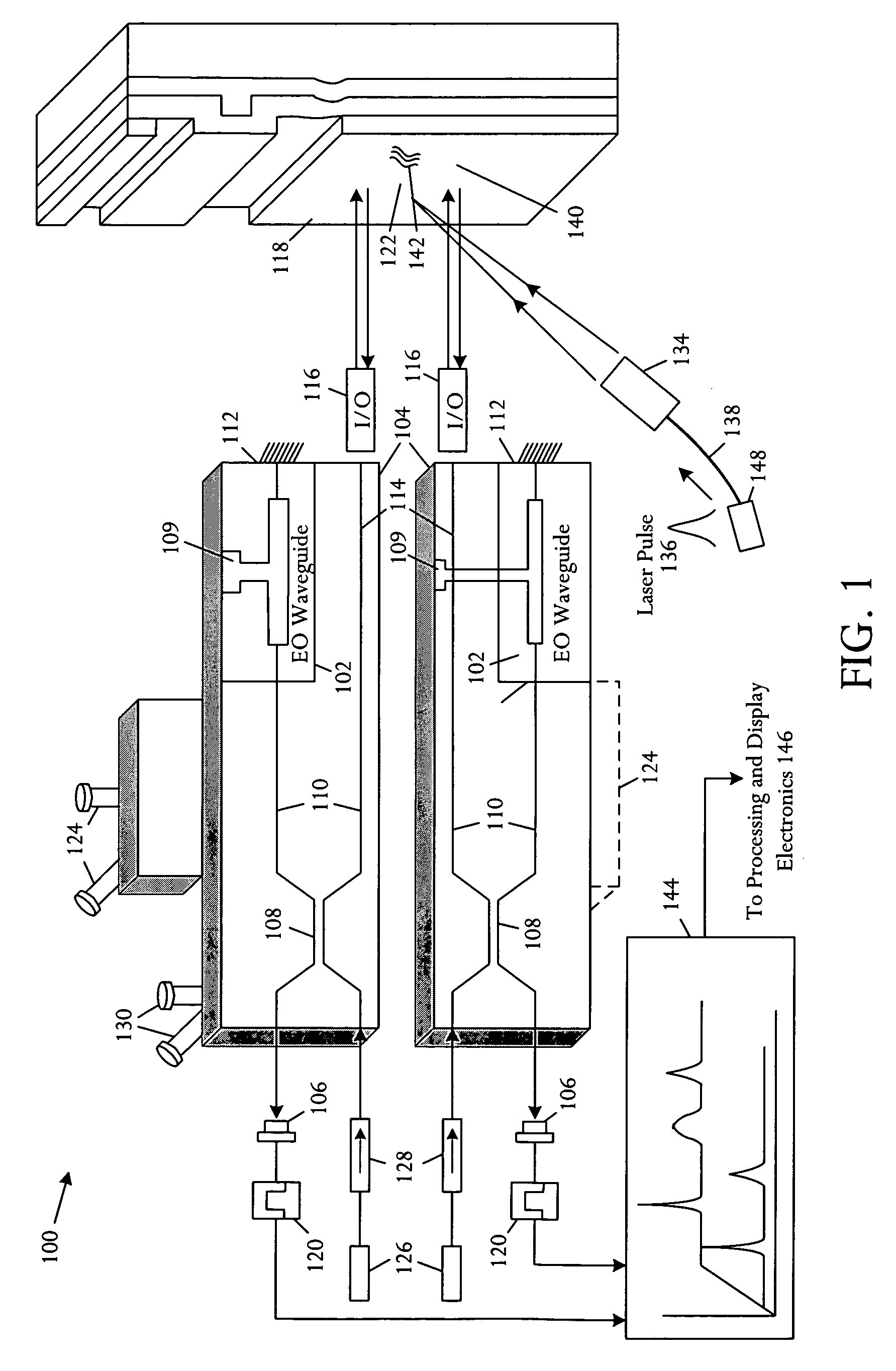
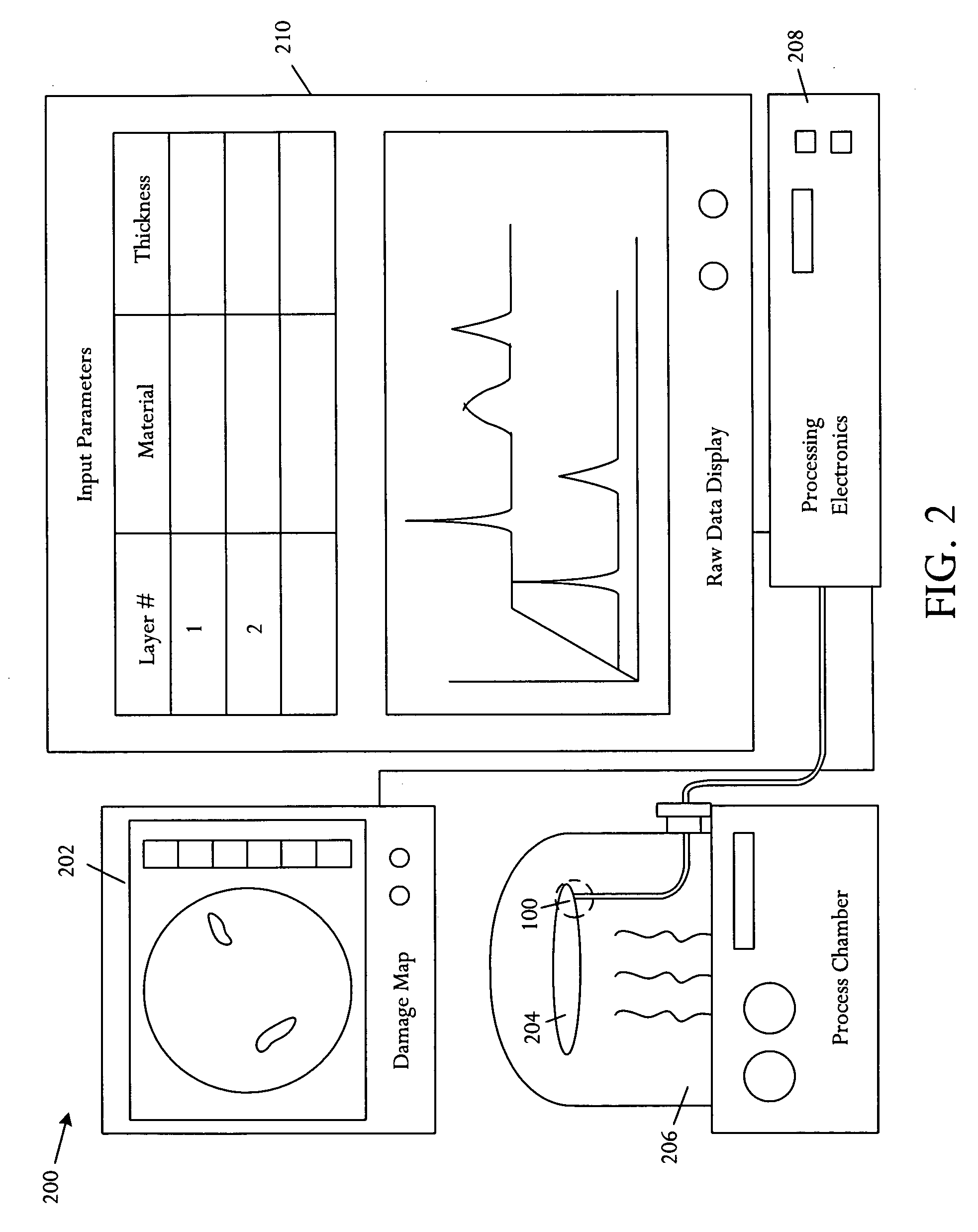
Sensors in various configurations and arrangements use optical modulators, fiber-optics, and bulk-optic interferometers to perform various measurements. In some applications, the various sensors detect pulsed laser-induced high-frequency acoustic resonance in a multi-layer material. The sensor down-converts high-frequency (GHz) acoustic signals to low-frequency (kHz) detectable signals. The resulting measurement may be either a single point defect signature or a two-dimensional (2D) acoustic “image” indicating subsurface defects. Defect examples include delamination, thickness variation, cracks, inclusions, and damaged micro- or nano-structure. Various architectures may be used for single point measurements and two-dimensional (2D) measurements, acquired in normal incidence and arbitrary angle of incidence measurements. The appended drawings depict several examples of suitable sensor structures.

The illustrative sensors and devices can be used for a variety of detection schemes. E...


PUM

PropertyMeasurementUnit
Sizeaaaaaaaaaa
Phaseaaaaaaaaaa
Frequencyaaaaaaaaaa

Abstract

A sensor comprises an optical modulator that generates a modulation signal, an interferometer that mixes an acoustic signal evoked by a pulsed laser with the modulation signal to down-convert the acoustic signal to lower frequencies, and a photodetector that detects the down-converted signal.

Description

BACKGROUND OF THE INVENTION Technical and economic factors continue to drive the evolution of semiconductor processing equipment. The semiconductor industry demands fabrication machines with a capability to process semiconductor wafers at high speed with substantial uniformity and reliability. Integrated circuit fabrication commonly involves numerous process steps with fabrication machinery processing semiconductor wafers at high speed to create structural features with high precision. Measurements are commonly made between process steps to verify features are within tolerances demanding a capability to perform non-destructive inspection and analysis of semiconductor wafers. Optical metrology is a highly useful technique for non-destructive analysis. Examples of optical metrology include ellipsometry, reflectometry, scatterometry, and others. Ellipsometry involves analysis of changes in polarization state of probe illumination. Reflectometry relates to analysis of changes in illum...

Claims


Application Information

Patent Timeline
IPC IPC(8): G01J1/00G01N29/24G01N29/30G01N29/46
CPCG01N29/2418G01N29/30G01N29/46G01N2291/0423G01N2291/015G01N2291/02491G01N2291/02827G01N2291/014
Inventor YACOUBIAN, ARAZ
Owner LER TECH
Why Eureka
Try Eureka