Semiconductor device and method for fabricating the same

a technology of semiconductor devices and semiconductor components, applied in the details of semiconductor/solid-state devices, semiconductor devices, electrical apparatus, etc., can solve the problems of degrading the reliability of semiconductor devices and increasing the problem of problems, and achieve the effect of high aspect ratio

Active Publication Date: 2005-02-03
PANNOVA SEMIC
View PDF4 Cites 37 Cited by
  • Summary
  • Abstract
  • Description
  • Claims
  • Application Information

AI Technical Summary

Benefits of technology

[0029] The semiconductor device according to the present invention and the fabrication method therefor also have the marked effect of allowing the formation of the low-defect tungsten plug in the hole with a high aspect ratio provided in the insulating film so that they are useful as a semiconductor device having a tungsten plug and a fabrication method therefor.

Problems solved by technology

In accordance with the method for fabricating the conventional semiconductor device, however, a problem is encountered that a tungsten-film burying defect occurs to form a seam (void) 107 in the contact hole 102, as shown in FIG. 10, which leads to the degradation of the reliability of the semiconductor device resulting from the defect.
The problem becomes more pronounced with the miniaturization of the contact hole or with the increase of the aspect ratio thereof.

Method used


Image

  • Semiconductor device and method for fabricating the same
  • Semiconductor device and method for fabricating the same
  • Semiconductor device and method for fabricating the same

Examples


Embodiment Construction

[0041] Referring now to the drawings, a semiconductor device according to an embodiment of the present invention and a fabrication method therefor will be described with reference to the drawings.

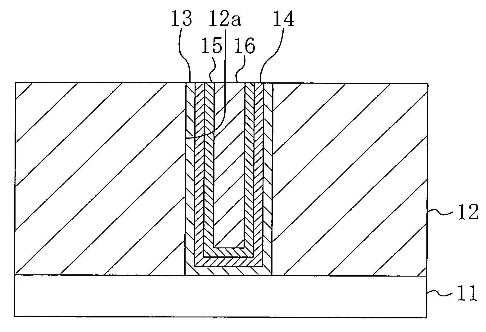
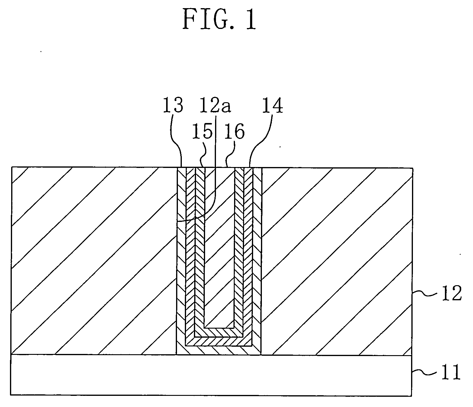
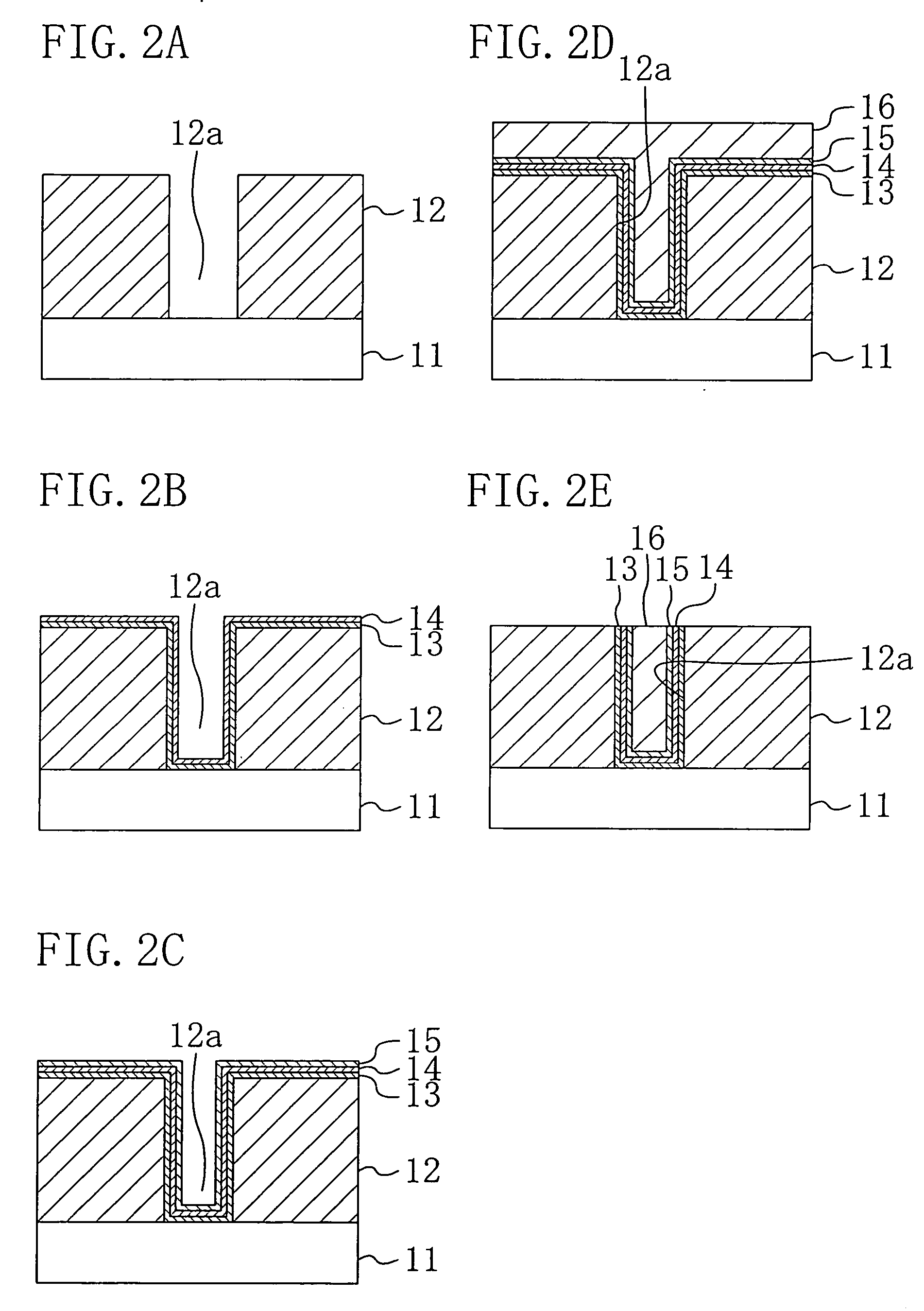
[0042]FIG. 1 shows a cross-sectional structure of the semiconductor device according to the embodiment of the present invention. As shown in FIG. 1, an insulating film 12 made of, e.g., a silicon oxide and having a thickness of about 1.5 μm is deposited on a semiconductor substrate 11 made of, e.g., silicon and having an upper surface provided with a semiconductor integrated circuit (not shown) including a semiconductor element and the like. The insulating film 12 is provided with a contact hole 12a reaching a portion of the upper surface of the semiconductor substrate 11, e.g., the semiconductor element. In the present embodiment, the diameter of the opening portion of the contact hole 12a is about 0.18 μm. A titanium film 13 with a thickness of, e.g., about 5.5 nm, a titanium nitride fil...


PUM

PropertyMeasurementUnit
diametersaaaaaaaaaa
opening diameteraaaaaaaaaa
diameteraaaaaaaaaa

Abstract

After forming a hole in an insulating film, a first tungsten film is formed over the wall and bottom surfaces of the hole. Then, a second tungsten film is formed by using the first tungsten film as a seed layer to fill up the hole. When the first tungsten film is formed, the average value of the diameters of crystal grains of the portion of the first tungsten film which is formed on the bottom surface of the hole is suppressed to 30 nm or less.

Description

BACKGROUND OF THE INVENTION [0001] The present invention relates to a semiconductor device and a method for fabricating the same and, more particularly, to a semiconductor device in which a tungsten plug is provided on a semiconductor element or a wire and a method for fabricating the same. [0002] Conventionally, a tungsten plug provided to extend through an insulating film has been used as an electrode for supplying a current and a signal to a semiconductor element or a lower layer wire covered with the insulating film (see, e.g., Japanese Laid-Open Patent Publication No. 2001-60564). [0003]FIG. 9 shows a cross-sectional structure of a conventional semiconductor device having a tungsten plug. As shown in FIG. 9, an insulating film 102 made of a silicon oxide is formed on a semiconductor substrate 101 made of silicon and having an upper surface provided with a semiconductor integrated circuit (not shown) including a semiconductor element and the like. The insulating film 102 is form...

Claims


Application Information

Patent Timeline
Patent Type & Authority Applications(United States)
IPC IPC(8): H01L21/285H01L21/44H01L21/768H01L23/52
CPCH01L21/28556H01L21/76862H01L21/76877H01L21/76876H01L21/76864
Inventor NISHIMURA, ATSUSHIHINOMURA, TORUIKEDA, ATSUSHIKISHIDA, TAKENOBU
Owner PANNOVA SEMIC
Why Eureka
Try Eureka