Processing apparatus for object to be processed and processing method using same

a processing apparatus and processing method technology, applied in the direction of coatings, chemical vapor deposition coatings, metallic material coating processes, etc., can solve the problems of dielectric breakdown of various fine devices, damage to the wafer itself, and generation of particles

Inactive Publication Date: 2005-02-17
TOKYO ELECTRON LTD
View PDF23 Cites 394 Cited by
  • Summary
  • Abstract
  • Description
  • Claims
  • Application Information

AI Technical Summary

Problems solved by technology

Thus, the wafer itself is damaged by an impact, or particles are generated due to a collision between the wafer and an upper electrode.
For example, if the charge neutralization voltage is too high, a charge neutralization of the wafer is sufficiently performed and, thus, there is no jump-up of the wafer, whereas it may cause an dielectric breakdown of various fine devices formed on the semiconductor wafer due to a large electric field.
However, in the aforementioned eye observation, it is difficult to objectively judge an occurrence of the jump-up of the wafer due to individual variances and, thus, a same examination should be iteratively performed to obtain objectivity.
Further, since a state of the occurrence of the jump-up is different depending on, e.g., types of films formed on a wafer surface or there exist differences between individual processing apparatuses, a considerable time is required to search for an optimal charge neutralization voltage for every processing apparatus by judging whether or not the wafer jumps up or obtain conditions for the optimal charge neutralization voltage.

Method used


Image

  • Processing apparatus for object to be processed and processing method using same
  • Processing apparatus for object to be processed and processing method using same
  • Processing apparatus for object to be processed and processing method using same

Examples


Embodiment Construction

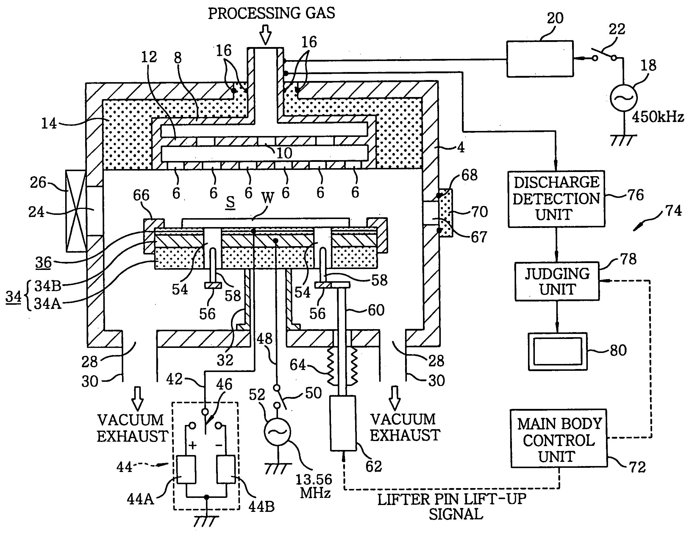
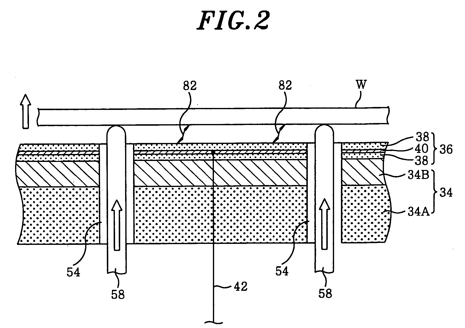
[0020] Hereinafter, a processing apparatus for an object to be processed and a processing method in accordance with the present invention will be described. FIG. 1 shows a processing apparatus for an object to be processed, which processes a semiconductor wafer; FIG. 2 illustrates a fragmentary enlarged view for explaining a discharge status generated when a semiconductor wafer is lifted up to be separated from the susceptor; FIG. 3 describes a flowchart for explaining a jump-up detection method of the present invention; and FIG. 4 depicts a relationship between a charge neutralization voltage and an occurrence of a discharge.

[0021] Above all, an exemplary processing apparatus for an object to be processed (e.g. wafer) in accordance with the present invention will be described.

[0022] As illustrated, a processing apparatus 2 includes a cylindrical processing vessel 4 made of, e.g., nickel or nickel alloys; and a susceptor 34 installed in the processing vessel 4, for mounting thereo...


PUM

PropertyMeasurementUnit
discharge voltageaaaaaaaaaa
frequencyaaaaaaaaaa
frequencyaaaaaaaaaa

Abstract

A processing apparatus includes a processing vessel; a susceptor installed in the processing vessel and having an electrostatic chuck for attracting and holding an object to be processed; lifter pins, elevatably installed with respect to the susceptor, for separating the object from the susceptor; and a jump-up detection device for detecting whether or not the object jumps up from the susceptor when the object is lifted up to be separated therefrom by the lifter pins, wherein the jump-up detection device has a discharge detection unit for detecting at least one of a discharge current and a discharge voltage generated between the object and the susceptor when the object is separated from the susceptor; and a judging unit for judging whether or not the object jumps up based on a detection result of the discharge detection unit.

Description

[0001] This application is a Continuation Application of PCT International Application No. PCT / JP03 / 03648 filed on Mar. 25, 2003, which designated the United States.FIELD OF THE INVENTION [0002] The present invention relates to a processing apparatus for an object to be processed and a processing method, which are capable of automatically detecting whether or not a semiconductor wafer jumps up when the semiconductor wafer is separated from a susceptor in a processing apparatus for a semiconductor wafer or the like using an electrostatic chuck. BACKGROUND OF THE INVENTION [0003] Generally, a processing apparatus such as a plasma etching apparatus, a plasma CVD apparatus, a plasma sputtering apparatus or the like includes a susceptor for mounting thereon a semiconductor wafer and a thin electrostatic chuck installed on the susceptor, wherein the semiconductor wafer is actually mounted on a surface of the electrostatic chuck. Further, a DC positive high voltage is continuously applied ...

Claims


Application Information

Patent Timeline
Patent Type & Authority Applications(United States)
IPC IPC(8): H01L21/00H01L21/683H01L21/3065
CPCH01L21/6833H01L21/6831
Inventor ONO, KATSUHIKO
Owner TOKYO ELECTRON LTD
Why Eureka
Try Eureka